
Semiconductor device and method of forming the same as well as a photo-mask used therein

a technology of mimiconductor and mask, which is applied in the field of mimiconductor devices and the same as the photo-mask used therein, can solve the problems of further reduction of capacity, difficult to compensate for the deformation of the mimiconductor pattern, and different resist patterns, etc., and achieves the effect of reducing occupied area, limiting or expanding capacity

Inactive Publication Date: 2005-03-03
RENESAS ELECTRONICS CORP
View PDF10 Cites 5 Cited by
  • Summary
  • Abstract
  • Description
  • Claims
  • Application Information

AI Technical Summary

Benefits of technology

The present invention provides a semiconductor device with capacitors that have a large capacity but a limited or reduced occupied area. This is achieved through the use of a novel method and photo-mask for forming a capacitor pattern. The invention also includes a resist pattern and a device pattern formed using the resist pattern. The technical effects of the invention include improved efficiency in semiconductor device production and reduced costs.

Problems solved by technology

This means that the resist pattern is different in shape from the photo-mask pattern due to the optical proximity effect, particularly if the pattern size is close to the limitation of the resolving power of the exposure system.
Even if each corner of the rectangular-shaped opaque pattern 100 extends outwardly for the purpose of compensation of the optical proximity effect, then the scaling down of the pattern makes it difficult to compensate for the deformation of the photo-resist pattern.
Particularly, in the capacitor under bit-line structure, it is essential to reduce the size of the pattern of the storage electrode for the purpose of securing a sufficient margin between the bit-contact and the storage electrode, resulting in further reduction in capacity.

Method used


Image

  • Semiconductor device and method of forming the same as well as a photo-mask used therein
  • Semiconductor device and method of forming the same as well as a photo-mask used therein
  • Semiconductor device and method of forming the same as well as a photo-mask used therein

Examples


Embodiment Construction

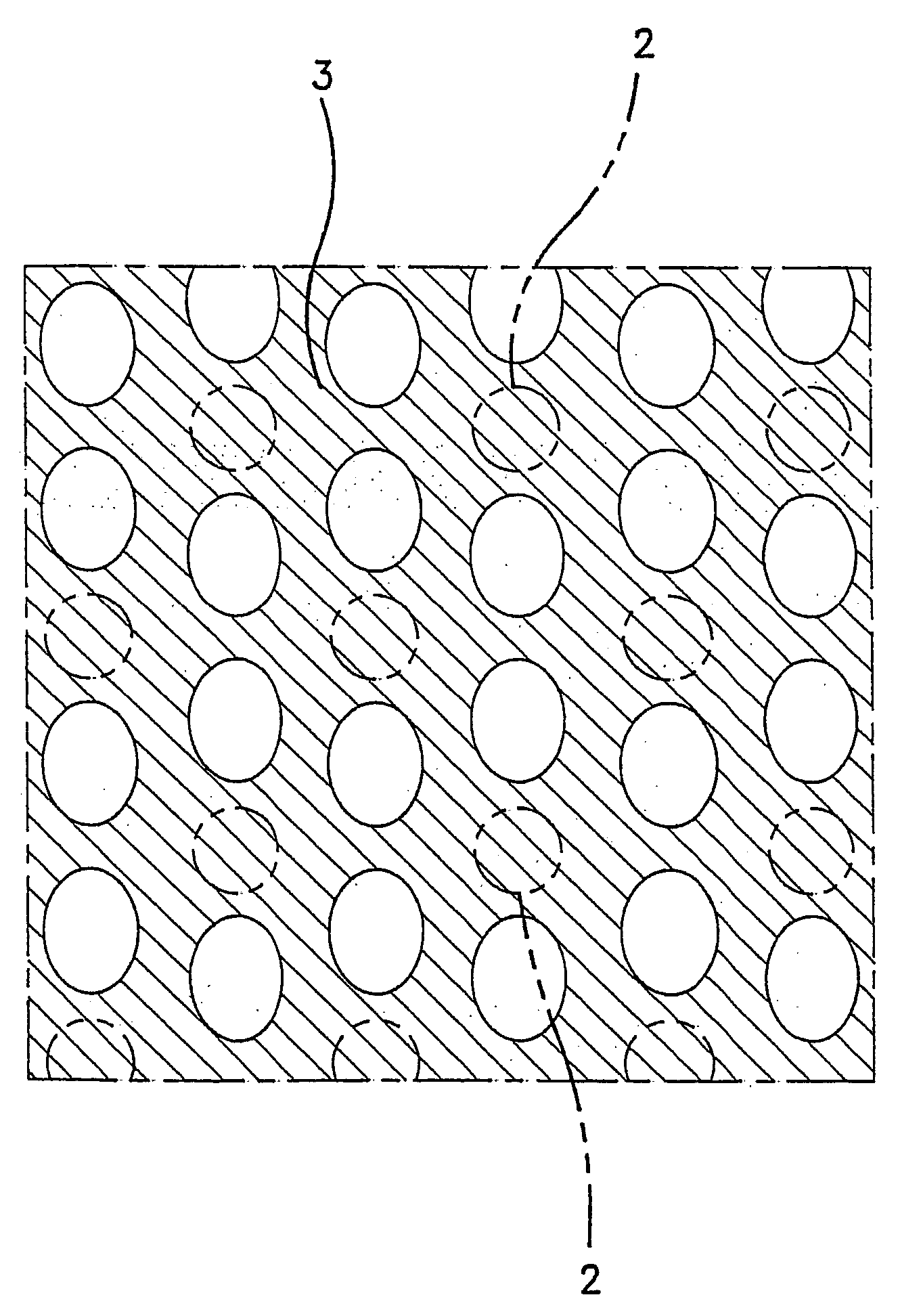
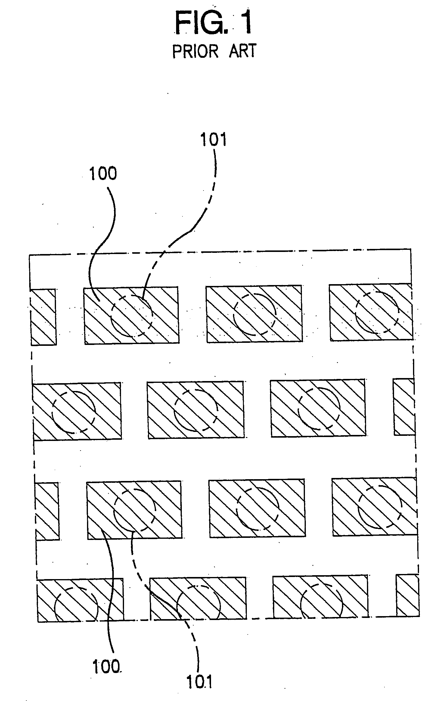
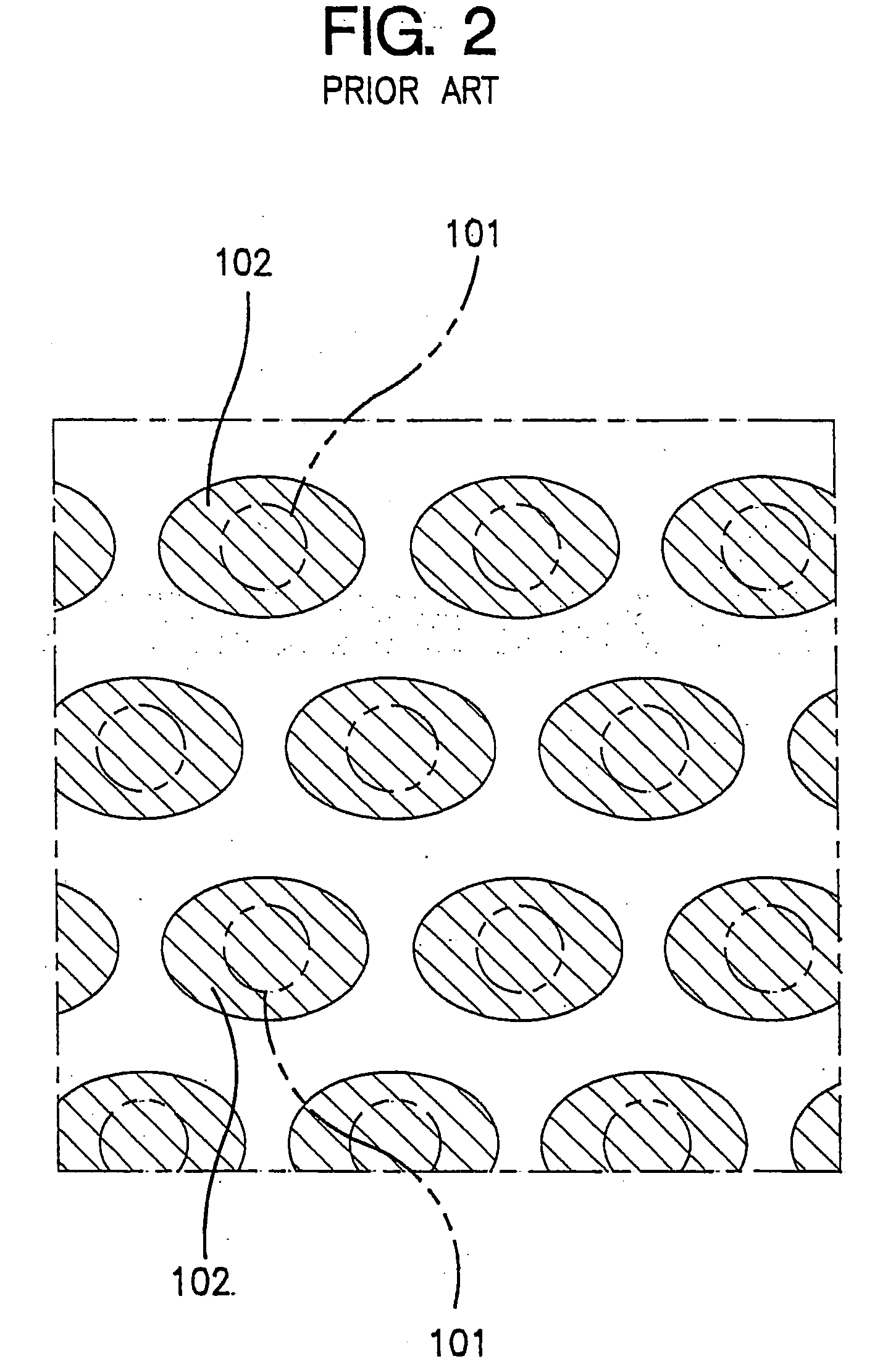
[0056] A first embodiment according to the present invention will be described in detail with reference to the drawings. FIG. 7A is a fragmentary plan view illustrative of a memory cell of a dynamic random access memory in a preferred embodiment in accordance with the present invention. FIG. 7B is a fragmentary cross sectional elevation view illustrative of the memory cell taken along an A-A line of FIG. 7A. FIG. 8 is a fragmentary plan[e] view illustrative of a memory cell array of the dynamic random access memory of FIG. 7A. FIG. 9 is a plan view illustrative of a photo-mask having mask-patterns to be used in an over-exposure process involved in a lithography process for forming storage electrode patterns of the memory cell array of FIG. 8.

[0057] With reference to FIG. 7B, a field effect transistor 12 is formed in a surface of a silicon substrate 11. A first inter-layer insulator 13 extends over the surface of the silicon substrate 11 and covers the field effect transistor 12. Th...


PUM

PropertyMeasurementUnit
distanceaaaaaaaaaa
wavelengthaaaaaaaaaa
transmissionaaaaaaaaaa

Abstract

A method of forming a device pattern of a semiconductor device. The method includes the steps of carrying out an over-exposure to a resist film using a mask which has transmission regions which are positioned about a circumference of each of intended patterns of a resist film. Then carrying out a development of the resist film to form a resist pattern having the intended patterns. And then forming a device pattern of a semiconductor device by use of the resist pattern.

Description

CROSS REFERENCE TO RELATED APPLICATIONS [0001] This application is a division of co-pending application Ser. No. 10 / 384,746, filed on Mar. 11, 2003, which is a division of U.S. application Ser. No. 09 / 546,528, filed Apr. 10, 2000. The entire contents of each of the above-identified applications are hereby incorporated by reference.[0002] The present invention relates to a semiconductor device having an improved pattern and a method of forming the same as well as a photo-mask used in the method of forming the semiconductor device, and more particularly to a method of forming a pattern for capacitors of dynamic random access memories needed to be increased in capacity but in a limited occupied area, and a method of forming the same as well as a photo-mask. [0003] The dynamic random access memory has memory cell arrays, each of which comprises a switching transistor and a capacitor. The requirement for an increase in the density of integration of the dynamic random access memory has be...

Claims


Application Information

Patent Timeline
Patent Type & Authority Applications(United States)
IPC IPC(8): H01L21/027G03F1/00G03F1/36G03F1/68H01L27/02H10B12/00
CPCG03F1/144H01L27/10852H01L27/10811H01L27/0207G03F1/36H10B12/312H10B12/033
Inventor TAKEUCHI, MAMI
Owner RENESAS ELECTRONICS CORP
Features
  • Generate Ideas
  • Intellectual Property
  • Life Sciences
  • Materials
  • Tech Scout
  • Unparalleled Data Quality
  • Higher Quality Content
  • 60% Fewer Hallucinations
Learn More