Method for preventing contact defects in interlayer dielectric layer

a dielectric layer and interlayer technology, applied in the field of semiconductor/solid-state device manufacturing, can solve the problems of poor etching profile and etching defect in the substrate, serious obstacle in the alignment between each patterned layer, so as to improve the moisture absorption of the interlayer dielectric layer and increase the thermal stability of the dielectric layer

Active Publication Date: 2005-03-03
NAN YA TECH
View PDF7 Cites 9 Cited by
  • Summary
  • Abstract
  • Description
  • Claims
  • Application Information

AI Technical Summary

Benefits of technology

[0010] Accordingly, an object of the present invention is to provide a method of forming an interlayer dielectric (ILD) layer, which employs a plasma treatment performed on a dielectric layer containing boron and phosphorous and a capping layer in-situ formed overlying the dielectric layer, thereby improving moisture absorption in the interlayer dielectric layer and increasing thermal stability of the dielectric layer containing boron and phosphorous.
[0011] Another object of the present invention is to provide a method for preventing formation of etching defects in a contact, which employs a plasma treatment performed on a dielectric layer containing boron and phosphorous and a capping layer in-situ formed overlying the dielectric layer before the dielectric layer is etched, thereby preventing etching defects formed in the contact to increase device yield.
[0015] According to another object of the invention, a method for preventing formation of etching defects in a contact is provided. First, a BPSG layer is formed overlying a substrate. Next, a plasma treatment is performed on the BPSG layer. Next, a USG layer is formed in-situ overlying the BPSG layer to serve as an ILD layer with the BPSG layer. Next, a reflow process is performed on the ILD layer. The ILD layer is then etched to form at least one contact opening therein to expose the surface of the substrate. Finally, the contact opening is filled with a conductive plug.

Problems solved by technology

As semiconductor device geometries continue to decrease in size to provide more devices per fabricated wafer and faster devices, misalignment between each patterned layer is a serious obstacle.
However, since the thermal stability of the BPSG layer 108 is poor and the BPSG layer 108 easily reacts with moisture, poor etching profiles and etching defects occur in the substrate contact 110 after subsequent lithography and etching, as indicated by the arrow “a” shown in the FIG. 1b.

Method used


Image

  • Method for preventing contact defects in interlayer dielectric layer
  • Method for preventing contact defects in interlayer dielectric layer
  • Method for preventing contact defects in interlayer dielectric layer

Examples


Embodiment Construction

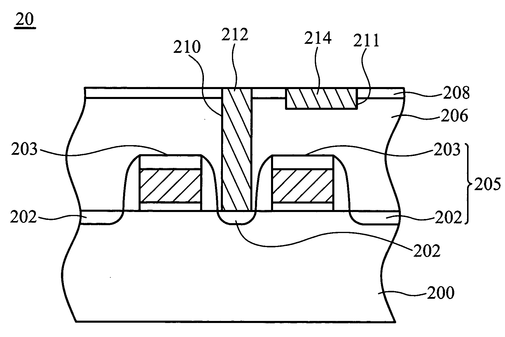
[0021]FIGS. 2a to 2d are cross-sections showing a method of forming a substrate contact (Cs) for a memory device, such as a dynamic random access memory (DRAM), according to the invention.

[0022] First, in FIG. 2a, a substrate 200, such as a silicon substrate or other semiconductor substrate, is provided. The substrate 200 may contain any semiconductor devices, such as MOS transistors, and capacitors, used in the memory devices. Here, in order to simplify the diagram, only a flat substrate is depicted. Moreover, the substrate 200 has a peripheral circuit region 20.

[0023] Next, a plurality of transistors 205 composed of gate structures 203 and source / drain doping regions 202 is formed on the peripheral circuit region 20. The gate structure 203 is composed of a gate dielectric layer, a gate, a gate capping layer, and a gate spacer. The gate dielectric layer may be a silicon oxide layer formed by thermal oxidation. The gate may be a single polysilicon layer or a composite layer compos...


PUM

PropertyMeasurementUnit
temperatureaaaaaaaaaa
dielectricaaaaaaaaaa

Abstract

A method of forming an interlayer dielectric (ILD) layer. A dielectric layer containing boron and phosphorous is formed overlying a substrate. A plasma treatment is subsequently performed on the dielectric layer using argon or nitrogen as a process gas. A capping layer is formed in-situ overlying the dielectric layer to serve as the ILD layer with the dielectric layer. A reflow process is subsequently performed on the ILD layer. A method for preventing formation of etching defects in a contact is also disclosed.

Description

BACKGROUND OF THE INVENTION [0001] 1. Field of the Invention [0002] The present invention relates in general to a semiconductor process, and more particularly, to a method of forming an interlayer dielectric (ILD) layer and a method for preventing formation of etching defects in a contact. [0003] 2. Description of the Related Art [0004] As semiconductor device geometries continue to decrease in size to provide more devices per fabricated wafer and faster devices, misalignment between each patterned layer is a serious obstacle. Therefore, many self-aligned processes have been developed in order to prevent misalignment and decrease the interval between devices, thereby increasing the device density. [0005]FIGS. 1a to 1c are cross-sections showing a conventional method of forming a substrate contact (Cs) for a memory device. First, in FIG. 1a, a silicon substrate 100, is provided. The substrate 100 may contain any semiconductor device, such as MOS transistors, and capacitors, used in t...

Claims


Application Information

Patent Timeline
Patent Type & Authority Applications(United States)
IPC IPC(8): H01L21/3105H01L21/316H01L21/768
CPCH01L21/02129H01L21/0234H01L21/02362H01L21/3105H01L21/76829H01L21/31625H01L21/76802H01L21/76819H01L21/76826H01L21/31612
Inventor TZOU, KAAN-LUCHEN, YAN-HONGCHEN, YI-NANWU, CHANG-RONG
Owner NAN YA TECH
Why Eureka
Try Eureka