Semiconductor device having a thin film capacitor and method for fabricating the same

a technology of thin film capacitor and semiconductor device, which is applied in the direction of transistors, coatings, instruments, etc., can solve the problems of high temperature process, deterioration of transistors in logic section, and inability to raise process temperature, and achieve small leakage current and large capacitance

Inactive Publication Date: 2005-03-10
IIZUKA TOSHIHIRO +3
View PDF14 Cites 49 Cited by
  • Summary
  • Abstract
  • Description
  • Claims
  • Application Information

AI Technical Summary

Benefits of technology

[0022] Another object of the present invention is to provide a capacitor which can realize a large capacitance and a small leakage current as a capacitor for a DRAM cell in a memory section of a semiconductor device having the memory section...

Problems solved by technology

Therefore, in a process after formation of the cobalt silicide layer, the process temperature cannot be elevated.
Accordingly, if Ta2O5 is used to form a capacitor dielectric film in the memory section of the logic mixed DRAM and if a polysilicon layer is used to form a lower capacitor electrode, a high temperature process is required to form the polysilicon layer, with the result that the transistors in the logic section become deteriorated through the high temperature process.
Therefore, in the generation of the gate length of 0.15 micron and in succeeding generations, it is not possible to use the polysilicon for the lower capacitor electrode.
However, a resonance frequency of the laminated ceramic capacitor is on the order of about 80 MHz, and therefore, when the LSI is speeded up to several hundred MHz to several GHz, a satisfactory electric charge compensation cannot be carried out, so that it does not function as the decoupling capacitor.
As a result, even if the thickness of the Ta2O5 film is reduced, a large capacitance cannot be obtained.
In addition, because of the oxidation occurring in the post anneal, a concavo-convex or a pe...

Method used


Image

  • Semiconductor device having a thin film capacitor and method for fabricating the same
  • Semiconductor device having a thin film capacitor and method for fabricating the same
  • Semiconductor device having a thin film capacitor and method for fabricating the same

Examples


first embodiment

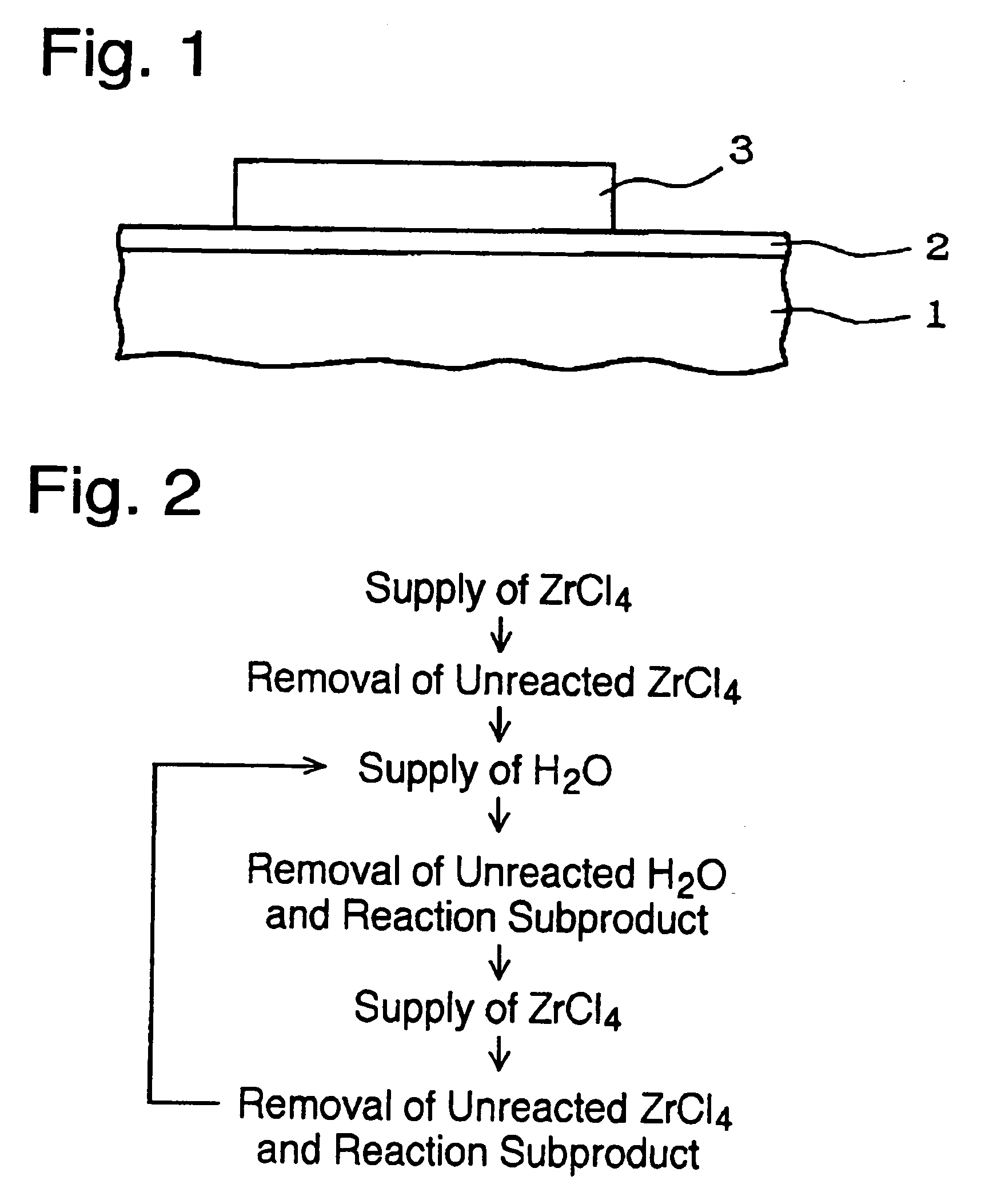
[0049] The first embodiment is a thin film capacitor of a MIM (metal-insulator-metal) structure, provided in a semiconductor device. This thin film capacitor includes a lower electrode 1, a capacitor dielectric film 2 and an upper electrode 3 stacked in the named order. Each of the upper electrode 3 and the lower electrode 1 is formed of at least one material selected from the group consisting of a metal and a metal nitride, represented by TiN, Ti, W, WN, Pt, Ir, Ru. The capacitor dielectric film 2 is formed of at least one material selected from the group consisting of ZrO2, HfO2, (Zrx, Hf1-x)O2 (0y, Ti1-y)O2 (0z, Ti1-z)O2 (0k, Til, Hfm)O2 (01, m<1, k+l+m=1), and formed by means of an atomic layer deposition (abbreviated to “ALD”).

[0050] Here, (Zrx, Hf1-x)O2 (0y, Ti1-y)O2 (0z, Ti1-z)O2 (0k, Til, Hfm)O2 (0

[0051] Here, a method for forming the thin film capacitor in the case that the capacitor dielectric film is f...

second embodiment

[0068] Now, the present invention will be described.

[0069] According to this second embodiment, in a thin film capacitor of a MIM structure having a capacitor dielectric film formed of at least one material selected from the group consisting of ZrO2, HfO2, (Zrx, Hf1-x)O2 (0y, Ti1-y)O2 (0z, Ti1-z)O2 (0k, Til, Hfm)O2 (0

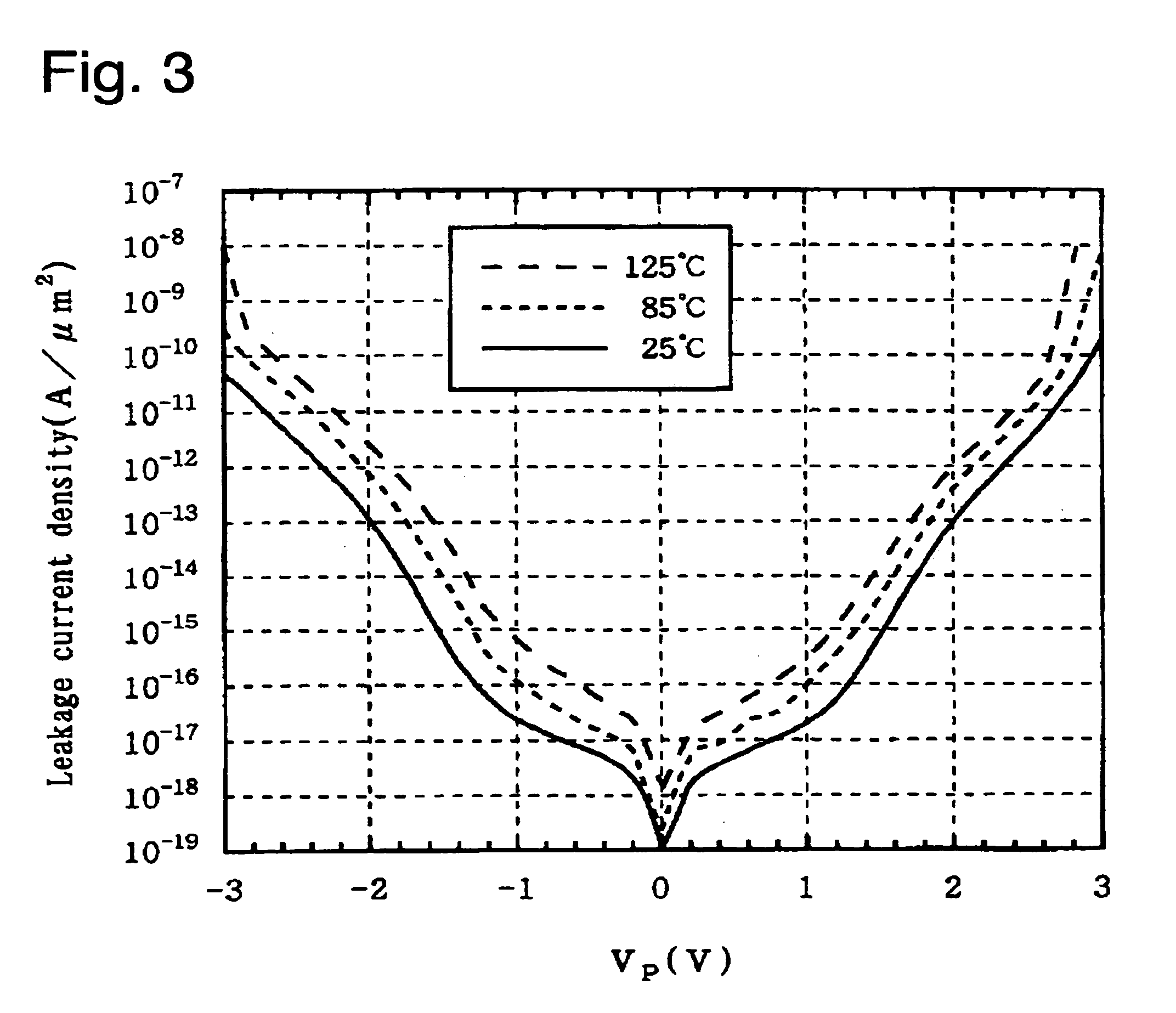
[0070] The thin film capacitor of the MIM structure in accordance with the first embodiment having the capacitor dielectric film formed of at least one material selected from the group consisting of ZrO2, HfO2, (Zrx, Hf1-x)O2 (0y, Ti1-y)O2 (0z, Ti1-z)O2 (0k, Til, Hfm)O2 (02O5, and therefore, can be satisfactorily used as a memory capacitor in a DRAM cell. However, when the film thickness of the capacitor dielectric film is decreased, the capacitance increase is small (namely, the decrease of teq is small), and on the other hand, the lea...

third embodiment

[0085] Now, the present invention will be described.

[0086] According to this third embodiment, in a stacked MIM (metal-insulator-metal) capacitor in a DRAM or a logic mixed DRAM having a logic section and a memory section formed on the same chip, a lower electrode, a capacitor dielectric film and an upper electrode are sequentially formed in the ALD process by use of an ALD apparatus.

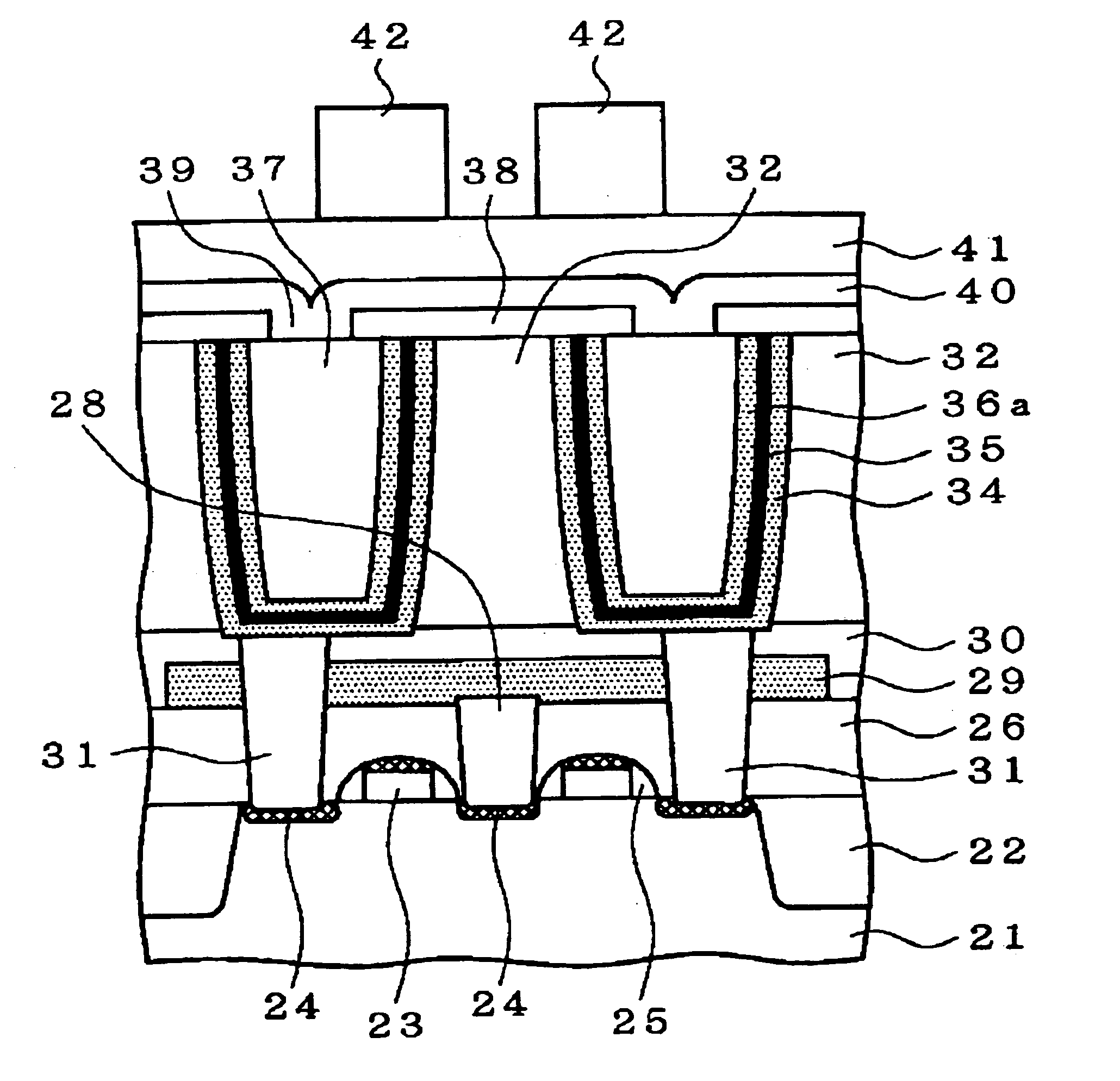
[0087] First, a conventional method for forming the stacked MIM capacitor in a DRAM or a logic mixed DRAM will be described. As shown in FIG. 7, a transistor is formed, and after a capacitor contact 11 is formed, an interlayer insulator film 12 is deposited. Then, an opening is formed in the interlayer insulator film 12 by use of lithography, and a lower electrode (metal) 13 is deposited. Thereafter, a resist 14 is filled into the opening to protect the opening, and only an upper portion of the interlayer insulator film is removed by an etch-back process or a CMP (chemical mechanical polishing) process...


PUM

PropertyMeasurementUnit
Nanoscale particle sizeaaaaaaaaaa
Temperatureaaaaaaaaaa
Dielectric polarization enthalpyaaaaaaaaaa

Abstract

In a thin film transistor, each of an upper electrode and a lower electrode is formed of at least one material selected from the group consisting of a metal and a metal nitride, represented by TiN, Ti, W, WN, Pt, Ir, Ru. A capacitor dielectric film is formed of at least one material selected from the group consisting of ZrO2, HfO2, (Zrx, Hf1-x)O2 (0<x<1), (Zry, Ti1-y)O2 (0<y<1), (Hfz, Ti1-z)O2 (O<z<l), (Zrk, Til, Hfm)O2 (0<k, l, m<1, k+l+m=1), by an atomic layer deposition process. The thin film transistor thus formed has a minimized leakage current and an increased capacitance.

Description

BACKGROUND OF THE INVENTION [0001] The present invention relates to a semiconductor device having a thin film capacitor and a method for fabricating the same. [0002] Heretofore, in a general purpose DRAM, Ta2O5 having a high dielectric constant has been considered as a capacitor dielectric film in a memory cell. In this case, it is an ordinary practice that a lower electrode of a capacitor is formed of a polysilicon layer which can be formed to have a concavo-convex surface (for example, so called HSG (hemi-spherical grain) structure) in order to increase a capacitance per a unitary area. In order to form this polysilicon layer, a high temperature process on the order of 700 to 900 degrees Celsius is required. [0003] On the other hand, in a logic mixed DRAM in which a logic section and a memory section are formed on the same chip, gate electrodes and source / drain diffused regions in the logic section are required to be provided with a cobalt (Co) silicide for a speedup of transistor...

Claims


Application Information

Patent Timeline
IPC IPC(8): C23C16/40C23C16/44C23C16/455H01L21/02H01L21/314H01L21/316H01L27/04H01L21/822H01L21/8242H01L27/108
CPCC23C16/405H01L21/0228G11C11/404G11C2207/104H01L21/3141H01L21/31604H01L21/31641H01L21/31645H01L27/10814H01L27/10852H01L27/10894H01L28/40H01L28/55H01L28/60H01L28/65H01L28/90H01L27/108H01L21/02181H01L21/02189H01L21/02194C23C16/45525H10B12/315H10B12/033H10B12/09H01L27/04H10B12/00
Inventor IIZUKA, TOSHIHIROYAMAMOTO, TOMOETODA, MAMIYAMAMICHI, SHINTARO
Owner IIZUKA TOSHIHIRO
Why Eureka
Try Eureka