Interconnect with composite barrier layers and method for fabricating the same

a technology of interconnection and barrier layer, which is applied in the direction of semiconductor/solid-state device manufacturing, basic electric elements, electric apparatus, etc., can solve the problems of low resistivity for faster signal propagation, loss of adhesion, delamination, etc., and achieve the effect of better adhesion

Active Publication Date: 2005-03-10
TAIWAN SEMICON MFG CO LTD
View PDF4 Cites 53 Cited by
  • Summary
  • Abstract
  • Description
  • Claims
  • Application Information

AI Technical Summary

Benefits of technology

[0012] One object of the present invention is to provide a b

Problems solved by technology

However, it has become more and more important that metal conductors that form the interconnections between devices as well as between circuits in a semiconductor have low resistivity for faster signal propagation.
However, copper implementation suffers from high diffusivity in common insulating materials such as silicon oxide, and oxygen-containing polymers, which causes corrosion of the copper with the attendant serious problems of loss of adhesio

Method used


Image

  • Interconnect with composite barrier layers and method for fabricating the same
  • Interconnect with composite barrier layers and method for fabricating the same
  • Interconnect with composite barrier layers and method for fabricating the same

Examples


first embodiment

[0026] First Embodiment

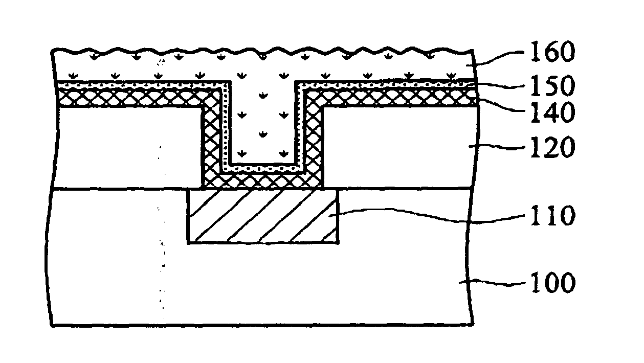
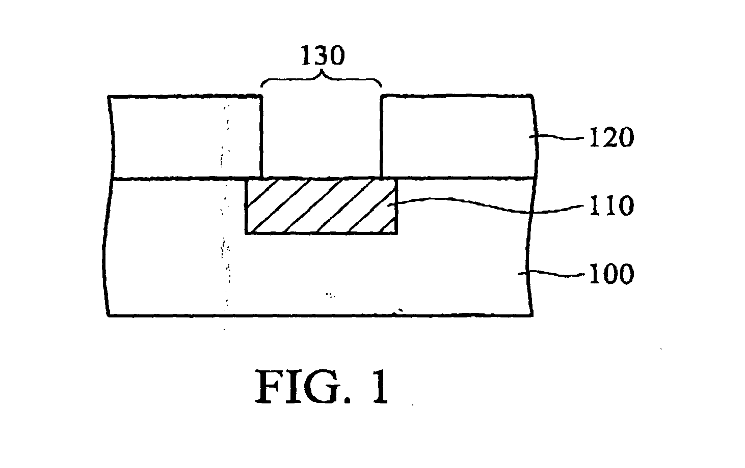
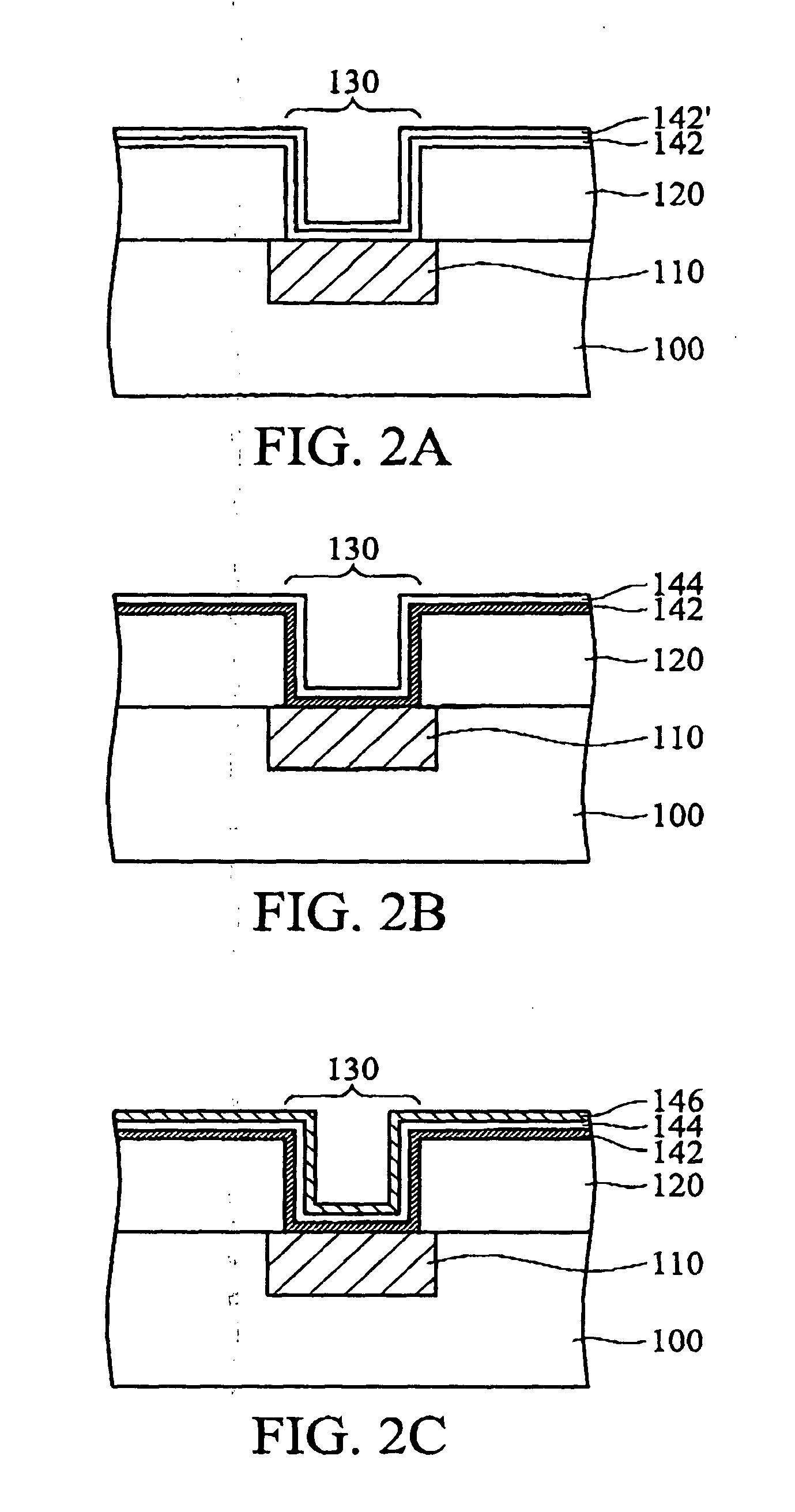
[0027]FIG. 1 shows a semiconductor substrate 100 such as a silicon substrate or silicon-on-insulator substrate (SOI). A contact region 110 is formed on the semiconductor substrate 100, such as a conventional MOS contact, interconnects and the like, which can be copper, aluminum, titanium, tantalum, tungsten, an alloy thereof, or a compound thereof.

[0028] As shown in FIG. 1, a dielectric layer 120 preferably having a planar upper surface is deposited overlying the substrate 100 and the contact region 110. The dielectric layer 120 is preferably composed of one or more dielectric depositions of silicon-containing or organic-based materials. Preferably, the dielectric layer 120 has a low dielectric constant (k), such as silicon oxide-containing material with a dielectric constant (k) not exceeding 3.5, more preferably 2.8 or below,. The preferred dielectric material is, but not limited to, organosilicate glass, fluorinated silica glass (FSG), organic spin-on glas...

second embodiment

[0040] Second Embodiment

[0041]FIG. 8 illustrates another embodiment of the invention, in which a two-level interconnect is formed by performing similar processes as in the first embodiment. As shown in FIG. 8, a low-k dielectric layer 120, e.g. k≦2.8, is deposited overlying a semiconductor substrate 100 with a first conductor 160 embedded therein. Preferably, a composite diffusion barrier layer 140 is interlaid between the conductor 160 and the first low-k dielectric layer 120, and the surface of the low-k dielectric layer 120 is below the surface of the first conductor 160 approximately 100 to 500 Å. An etch-stop layer 180 and a second low-k dielectric layer 190, e.g. k≦2.8, are deposited sequentially overlying the first dielectric layer 120. A second conductor 220 is embedded in the second low-k dielectric layer 190, connecting the underlying first conductor 160. The preferred width of the second conductor 220 is from 200 to 1000 Å. Preferably, a metal seed layer 210 and a composi...


PUM


Abstract

Composite ALD-formed diffusion barrier layers. In a preferred embodiment, a composite conductive layer is composed of a diffusion barrier layer and/or a low-resistivity metal layer formed by atomic layer deposition (ALD) lining a damascene opening in dielectrics, serving as diffusion blocking and/or adhesion improvement. The preferred composite diffusion barrier layers are dual titanium nitride layers or dual tantalum nitride layers, triply laminar of tantalum, tantalum nitride and tantalum-rich nitride, or tantalum, tantalum nitride and tantalum, formed sequentially on the opening by way of ALD.

Description

BACKGROUND OF THE INVENTION [0001] 1. Field of the Invention [0002] The present invention relates to semiconductor fabrication, and in particular to copper interconnects with improved diffusion barrier and adhesion between conductors and dielectrics, and methods for fabricating the same. [0003] 2. Description of the Related Art [0004] Aluminum and aluminum alloys were the most widely used interconnection metallurgies for integrated circuits. However, it has become more and more important that metal conductors that form the interconnections between devices as well as between circuits in a semiconductor have low resistivity for faster signal propagation. Copper is preferred for its low resistivity as well as for resistance to electromigration (EM) and stress voiding properties for very and ultra large scale integrated (VLSI and ULSI) circuits. [0005] Conventionally, copper interconnects are formed using a so-called “damascene” or “dual-damascene” fabrication process instead of convent...

Claims


Application Information

Patent Timeline
IPC IPC(8): H01L21/768
CPCH01L21/76846
Inventor YU, CHEN-HUATSENG, HORNG-HUEIJANG, SYUN-MINGHU, CHENMING
Owner TAIWAN SEMICON MFG CO LTD
Why Eureka
Try Eureka