

Semiconductor device
a technology of semiconductor devices and semiconductor films, applied in semiconductor devices, semiconductor/solid-state device details, electrical apparatus, etc., can solve the problems of high compression stress in al films, peeling, and risk of peeling, so as to reduce the compression stress of al films and prevent peeling. , the effect of high reliability
- Summary
- Abstract
- Description
- Claims
- Application Information
AI Technical Summary
Benefits of technology
Problems solved by technology
Method used
Image

Examples
embodiment 1
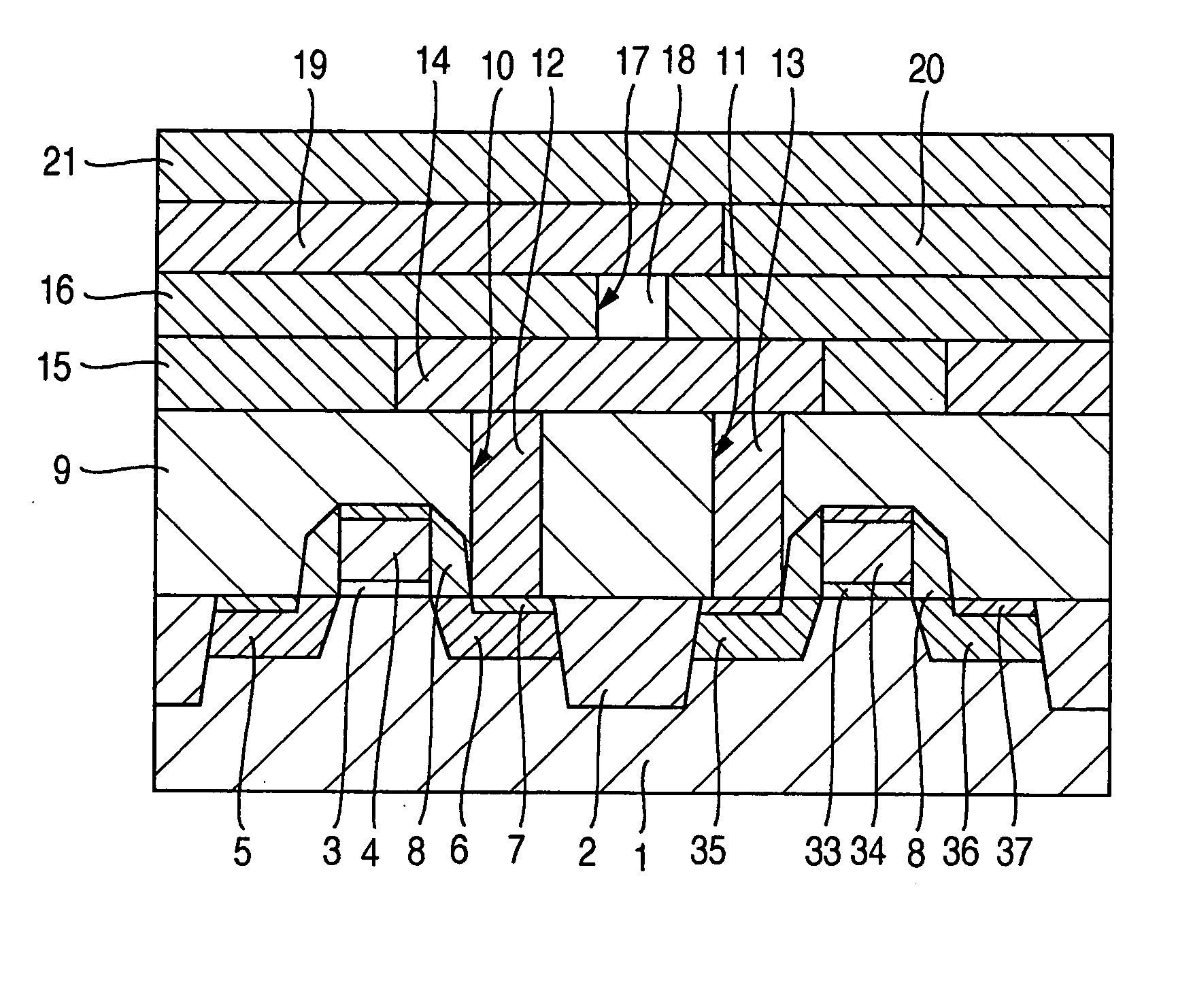
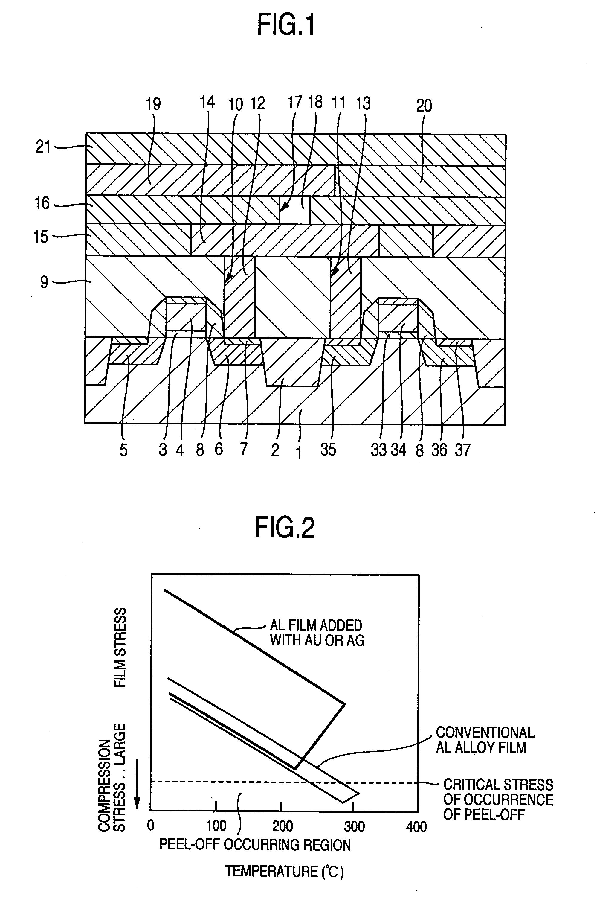
[0027]FIG. 1 is a schematic cross sectional view showing a main portion of a semiconductor device according to the embodiment 1.
[0028] As shown in FIG. 1, the semiconductor device of the embodiment 1 is constructed by using a p-type silicon substrate 1, as a main component, made of, for example, monocrystalline silicon as a semiconductor substrate. A plurality of element forming regions (active regions) partitioned by element separating regions 2 are formed on a principal plane (an element forming plane or a circuit forming plane) of the silicon substrate 1. For example, an MISFET (Metal Insulator Semiconductor Field Effect Transistor) is formed as a transistor element in each element forming region. In FIG. 1, the left side shows an n-channel conductivity type (n-type) MISFET and the right side shows a p-channel conductivity type (p-type) MISFET. The MISFET is a kind of insulating gate type field effect transistor. The MISFET whose gate insulating film is made of a silicon oxide f...
embodiment 2
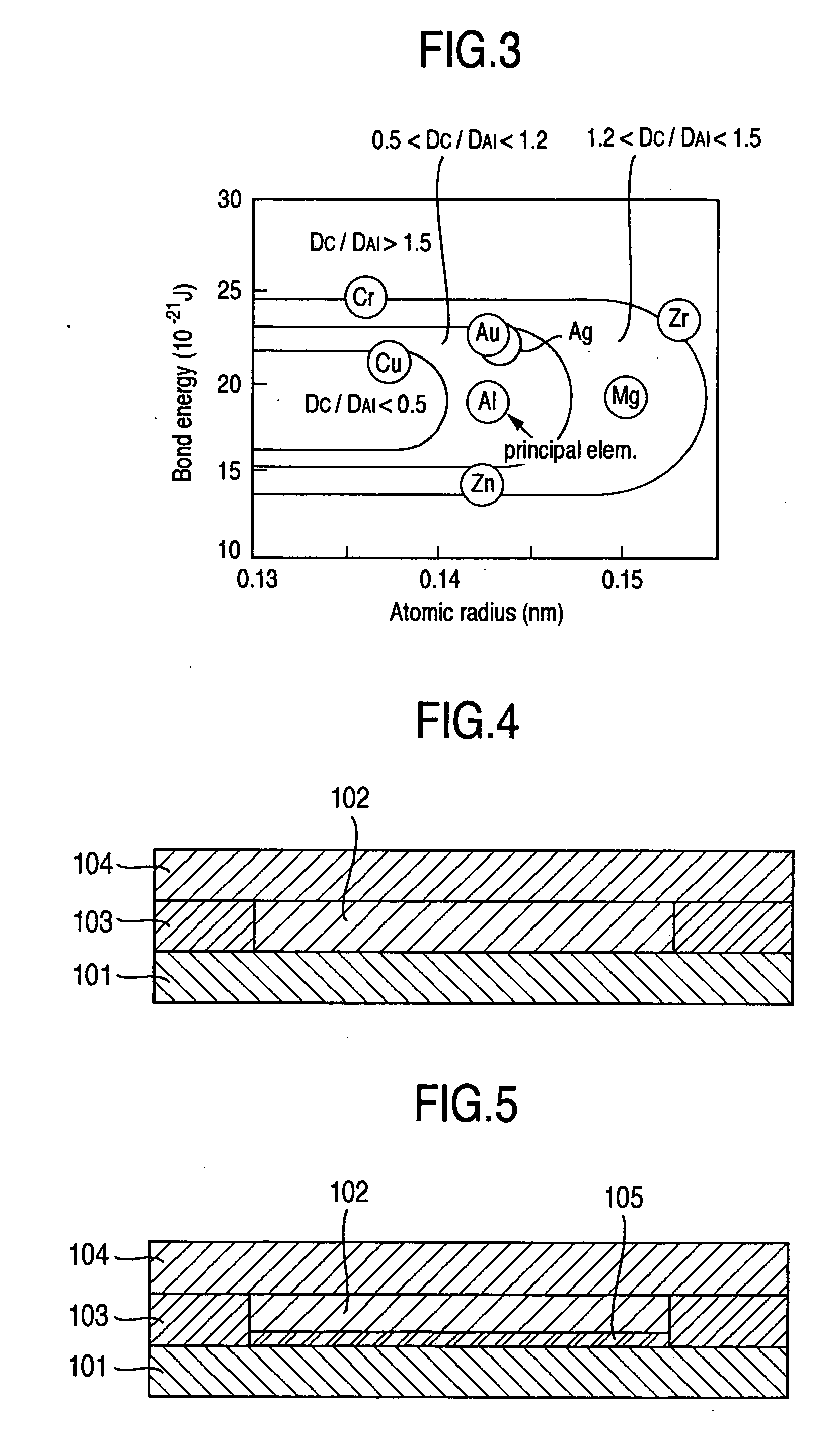
[0057] The embodiment 2 of the invention is shown in FIG. 4. FIG. 4 shows a wiring structure similar to that in the embodiment 1 shown in FIG. 1.
[0058] In the embodiment 2, the device has a structure in which an Al film 102 to which Au or Ag has been added is formed on an insulative material 101 and the whole surface of the Al film 102 to which Au or Ag has been added is covered with insulative materials 103 and 104. Thus, effects similar to those in the embodiment 1 mentioned above are obtained. By forming the wirings as a single layer of the Al film to which Au or Ag has been added, a semiconductor device of excellent manufacturing costs can be obtained without increasing the number of manufacturing steps.
[0059] Although the insulative material 101 is not limited to that shown here, it is made of, for example, a glass material such as BPSG, SOG, or the like in which SiO2 is used as a main component material, or a TEOS film, or silicon oxide, silicon nitride, or the like made by ...
embodiment 3
[0060] The embodiment 3 of the invention is shown in FIG. 5. FIG. 5 shows a modification of the wiring structure according to the invention. Component elements which are common to those in the embodiment 2 mentioned above are designated by the same reference numerals.
[0061] In the embodiment 3, a protecting film 105 is formed in a lower layer of the Al film 102 to which Au or Ag has been added. Another structure is similar to that in the embodiment 2 and effects similar to those in the embodiment 2 mentioned above are obtained. By providing the protecting film 105, such an effect of preventing the Al atoms from being diffused into the substrate or the like in the high-temperature heat treatment step is also obtained. By forming the protecting film 105 only to the lower layer of the Al film 102, there is such an advantage that the number of manufacturing steps is smaller and the manufacturing costs can be reduced more than those in the case where the protecting films are formed to t...
PUM
 Abstract
Description
Claims
Application Information