Stabilized OLED device
a technology of electroluminescent devices and stabilized oleds, which is applied in the direction of discharge tube luminescnet screens, other domestic articles, natural mineral layered products, etc., can solve the problems of inability to meet the requirements of many practical applications, the oled device emits color contaminating light, and the luminance output is gradually degraded, so as to improve efficiency and stability, improve stability and performance, and reduce angular dependence
- Summary
- Abstract
- Description
- Claims
- Application Information
AI Technical Summary
Benefits of technology
Problems solved by technology
Method used
Image
Examples
example 1
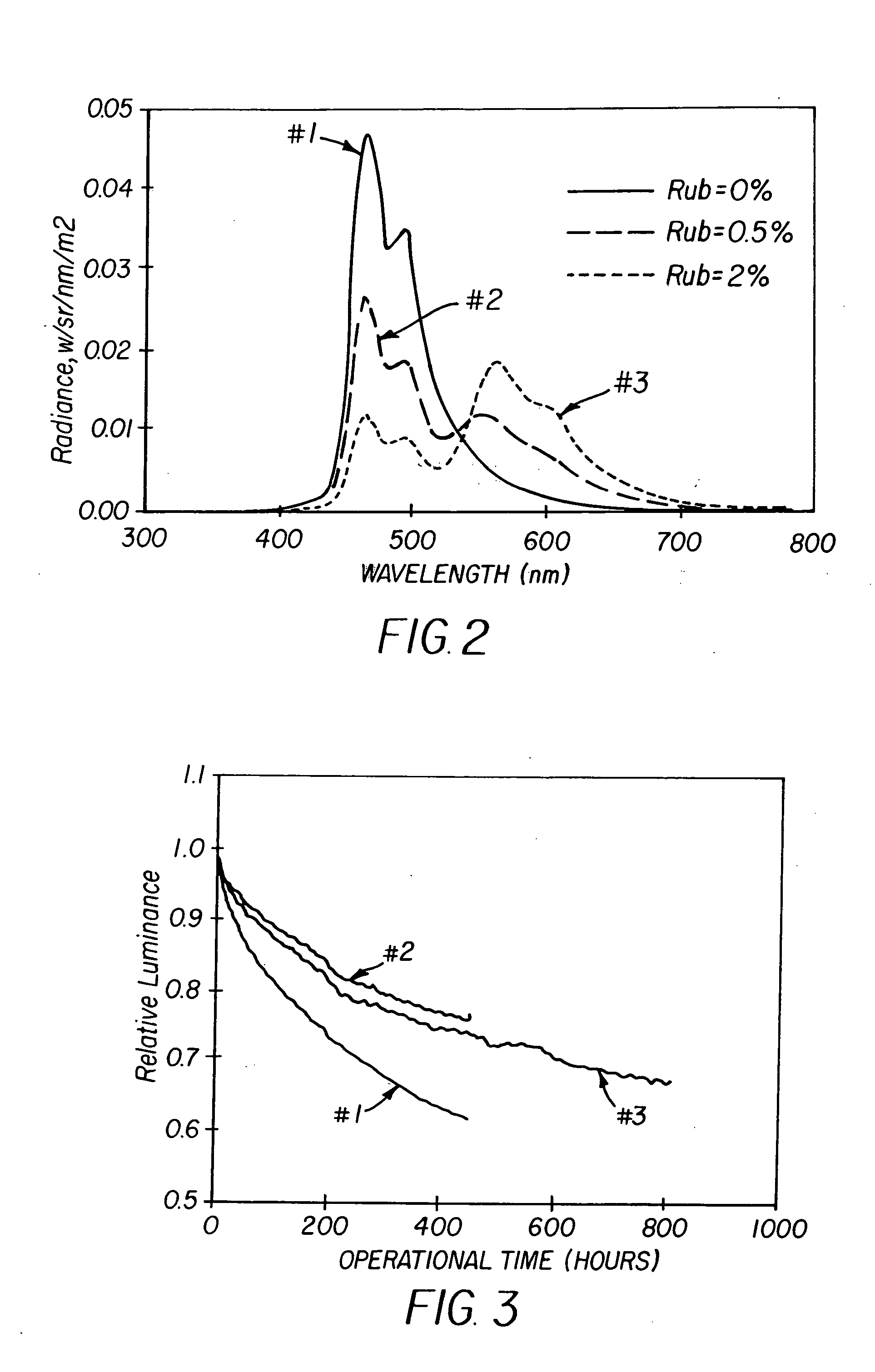
OLED devices #1, #2, and #3 were constructed in the following manner.
Substrates coated with 80 nm ITO were sequentially ultrasonicated in a commercial detergent, rinsed in deionized water, and degreased in toluene vapor. These substrates were treated with oxygen plasma for about one minute and coated with 1 nm fluorocarbon layer by plasma assisted deposition of CHF3. These substrates were loaded into a deposition chamber for organic layers and cathode depositions.
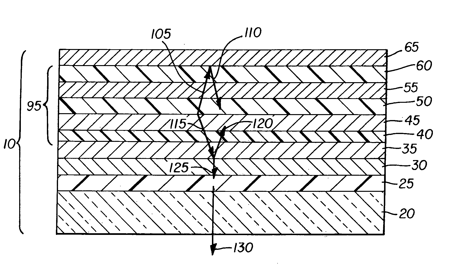
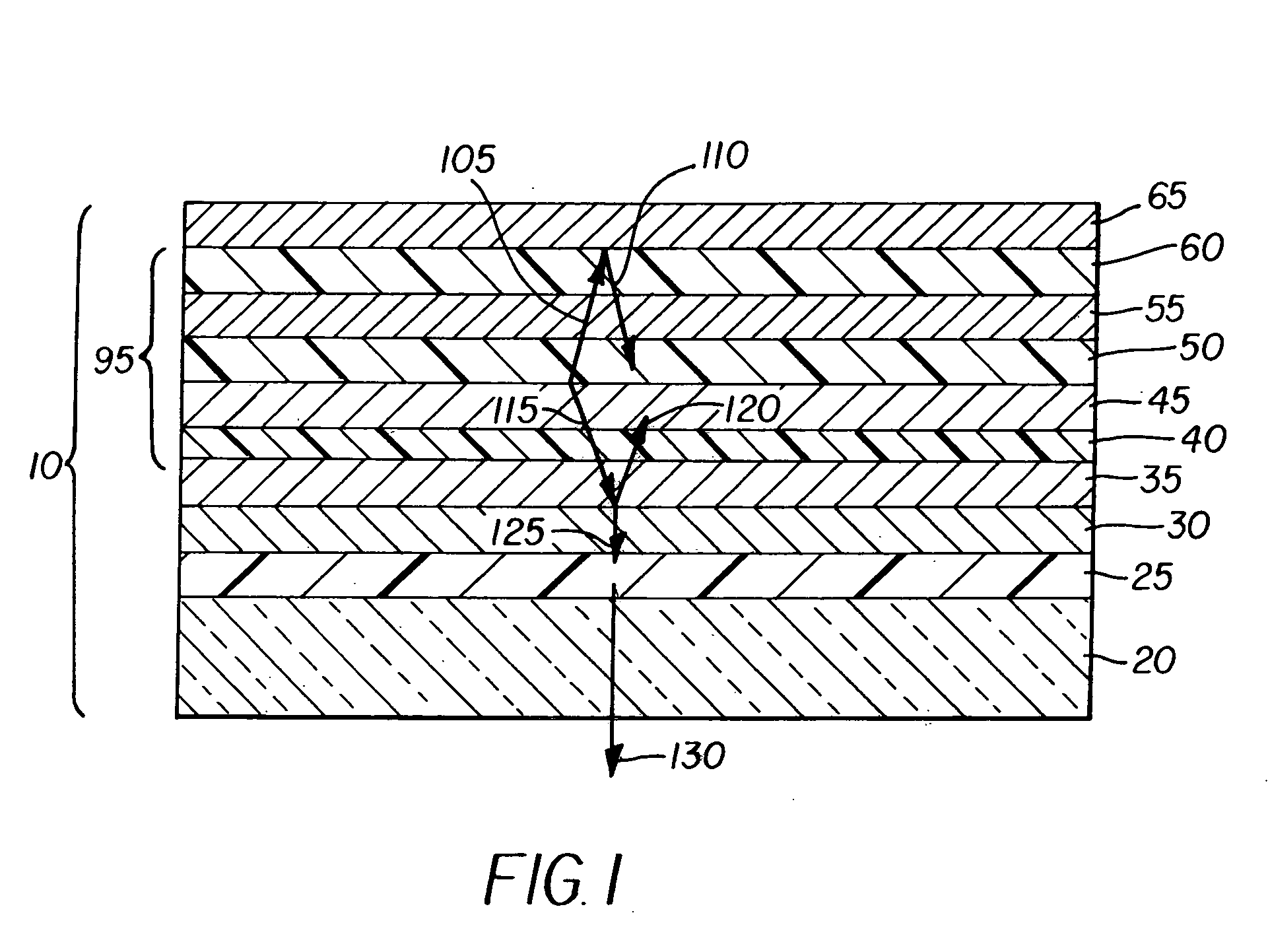
The devices of Example 1 were prepared by sequential deposition of 150 nm NPB hole-transport layer (HTL) doped with various amounts of rubrene, 20 nm blue emission layer (EML) comprising AND host with 1.5% TBP blue dopant, 35 nm Alq electron-transport layer (ETL), and 100 nm Mg:10% Ag alloy as the cathode. The above sequence completed the deposition of the OLED device. Device #1 had no rubrene doping into the HTL; device #2 had 0.5% of rubrene doped into the HTL; and device #3 had 2% rubrene doped into the HTL.
The OL...
example 2-a (comparative)
Oled devices #2-a was constructed in a manner similar to the samples in Example 1
A substrate coated with 40 nm ITO was sequentially ultrasonicated in a commercial detergent, rinsed in deionized water, and degreased in toluene vapor. This substrate was treated with oxygen plasma for about one minute and coated with 1 nm fluorocarbon layer by plasma assisted deposition of CHF3. The substrate was then loaded into a vacuum evaporation deposition chamber for sequential deposition of 87 nm of undoped NPB hole-transport layer (HTL), 20 nm of NPB hole-transport layer doped with 2.5% of rubrene, 30 nm blue emission layer (EML) comprising TBADN host with 1.5% TBP blue dopant, 32 nm Alq electron-transport layer (ETL), 0.5 nm Li electron injection layer, and 50 nm Ag alloy as the cathode. The above sequence completed the deposition of the OLED device. The OLED device was then hermetically packaged in a dry glove box filled with nitrogen for protection against ambient environment. The ITO pat...
PUM
 Abstract
Description
Claims
Application Information


