Formation of low resistance via contacts in interconnect structures

a technology of interconnect structure and contact, which is applied in the direction of basic electric elements, semiconductor/solid-state device manufacturing, electric apparatus, etc., can solve the problems of fatal ic failure mode, increased via resistance, and associated fabrication problems with prior art structures, and achieve low via contact resistance

Inactive Publication Date: 2005-03-24
GLOBALFOUNDRIES INC
View PDF5 Cites 23 Cited by
  • Summary
  • Abstract
  • Description
  • Claims
  • Application Information

AI Technical Summary

Benefits of technology

[0010] It is therefore an object of the present invention to provide methods of improved fabrication

Problems solved by technology

However, fabrication problems are associated with these prior art structures.
Another problem associated with these prior art structures is poor adhesion at the via contact, which leads to increased via resistance after the structure is cycled in temperature or after long periods of field operation.
The extreme case of increased via resistance is an open via with no contact to the line below, a fatal IC failure mode.
Poor adhesion is also due to the same contamination described above.
A further problem during interconnect

Method used


Image

  • Formation of low resistance via contacts in interconnect structures
  • Formation of low resistance via contacts in interconnect structures
  • Formation of low resistance via contacts in interconnect structures

Examples


Embodiment Construction

[0035] The present invention provides a non-destructive pre-clean process methods for liner / barrier deposition on low-k dielectrics.

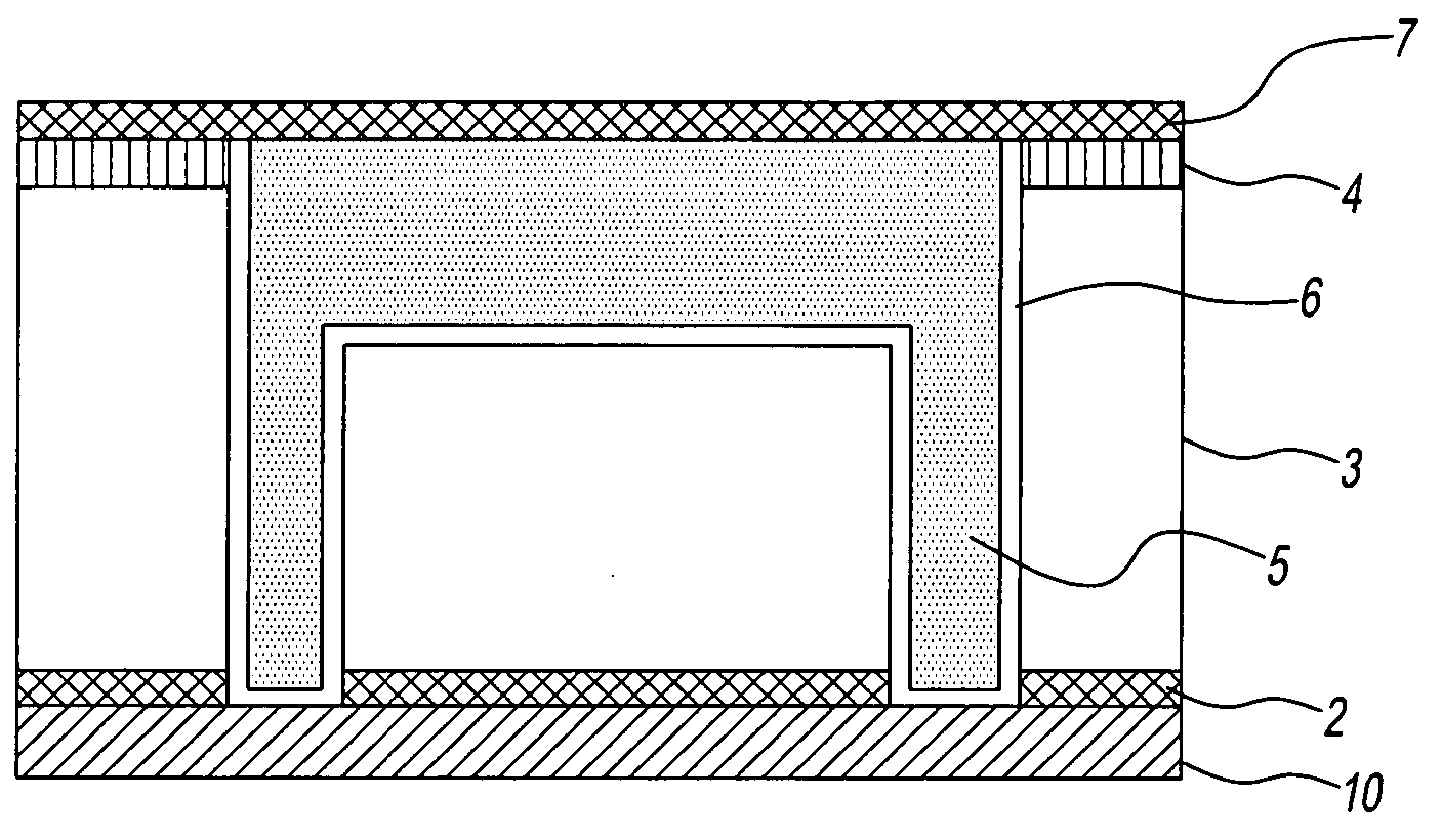
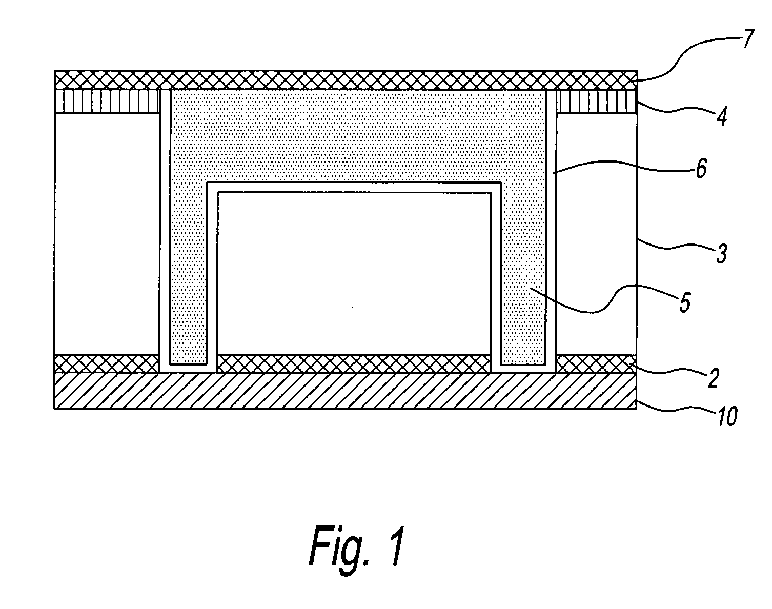
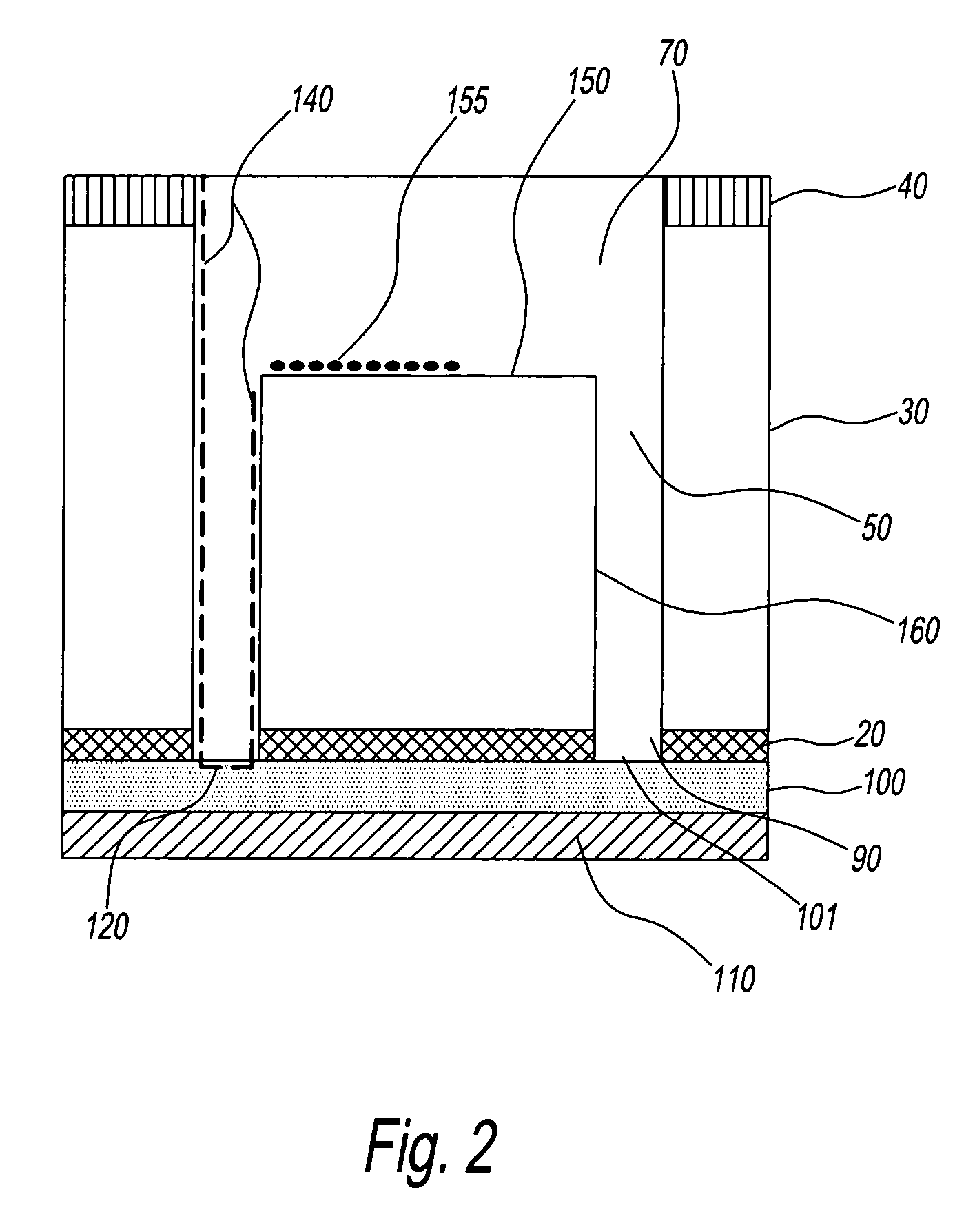
[0036] In general, an integrated circuit will have interconnect levels, each level including metallic lines and vias that are of a dual damascene (via plus next level conductor) wiring interconnect structure for use on the IC chip. The metallic lines and vias are composed of the same or different conductive material. Suitable materials for use herein include, but are not limited to, W, Cu, Al, Ag, Au and alloys thereof and the like. A particularly preferred material is Cu.

[0037] The condensable cleaning agent (CCA) can be a reducing agent; metal based reducing agent, metal hydride; mixed metal hydride such as, LiAIH, molecular source of fluorine or a source of hydrogen, or a source of both hydrogen and silicon.

[0038] Examples of the latter include, but are not limited to disilane; trisilane; tetrasilane and other condensable silanes.

[0039] Molecular...


PUM


Abstract

A method of fabricating an interconnect structure including the steps of: forming a porous or dense low k dielectric layer on a substrate; forming single or dual damascene etched openings in the low k dielectric; placing the substrate in a process chamber on a cold chuck at a temperature about −200° C. to about 25° C.; adding to the process chamber a condensable cleaning agent (CCA) to condense a layer of CCA within the etched openings on the substrate; and activating at a temperature about −200° C. to about 25° C. Also provided is an interconnect structure having a substrate, a conductive material disposed on the substrate, a porous or dense low k dielectric layer disposed on the conductive material, wherein the low k dielectric layer has a single or dual damascene etched openings that expose a surface of the conductive material, and metallic lines and vias etched onto the low k dielectric layer; wherein the exposed conductive material has been treated with a CCA and activated in the cold to remove oxide, oxygen and carbon containing residues from the surface of the conductive material.

Description

BACKGROUND OF THE INVENTION [0001] 1. Field of the Invention [0002] The present invention generally relates to integrated circuits (ICs). More particularly, the present invention relates to interconnect structures, including multilevel interconnect structures fabricated by damascene methods in which the via contact resistance must be low. The present invention describes various methods and tooling for making improved interconnect structures based on copper damascene wiring having a reduced via contact resistance and stable resistance both during IC operation and reliability stress of the IC device. [0003] 2. Description of the Prior Art [0004] Generally, semiconductor devices include a plurality of circuits, which form an integrated circuit fabricated on a silicon single crystal substrate. A complex network of signal paths will normally be routed to connect the circuit elements distributed on the surface of the substrate. Efficient routing of these signals across the device requires...

Claims


Application Information

Patent Timeline
IPC IPC(8): H01L21/306H01L21/311H01L21/768
CPCH01L21/02063H01L21/76814
Inventor DALTON, TIMOTHYGATES, STEPHEN
Owner GLOBALFOUNDRIES INC
Why Eureka
Try Eureka