

Solvent mixtures for an organic electronic device
a technology of organic electronic devices and solvent mixtures, which is applied in the manufacture of electrode systems, electric discharge tubes/lamps, discharge tubes luminescnet screens, etc., can solve the problems of photolithography techniques, large amount of materials consumed and wasted, and complicated steps, and achieves fast evaporation rate, low solubility, and high solubility.
- Summary
- Abstract
- Description
- Claims
- Application Information
AI Technical Summary
Benefits of technology
Problems solved by technology
Method used
Image

Examples
Embodiment Construction
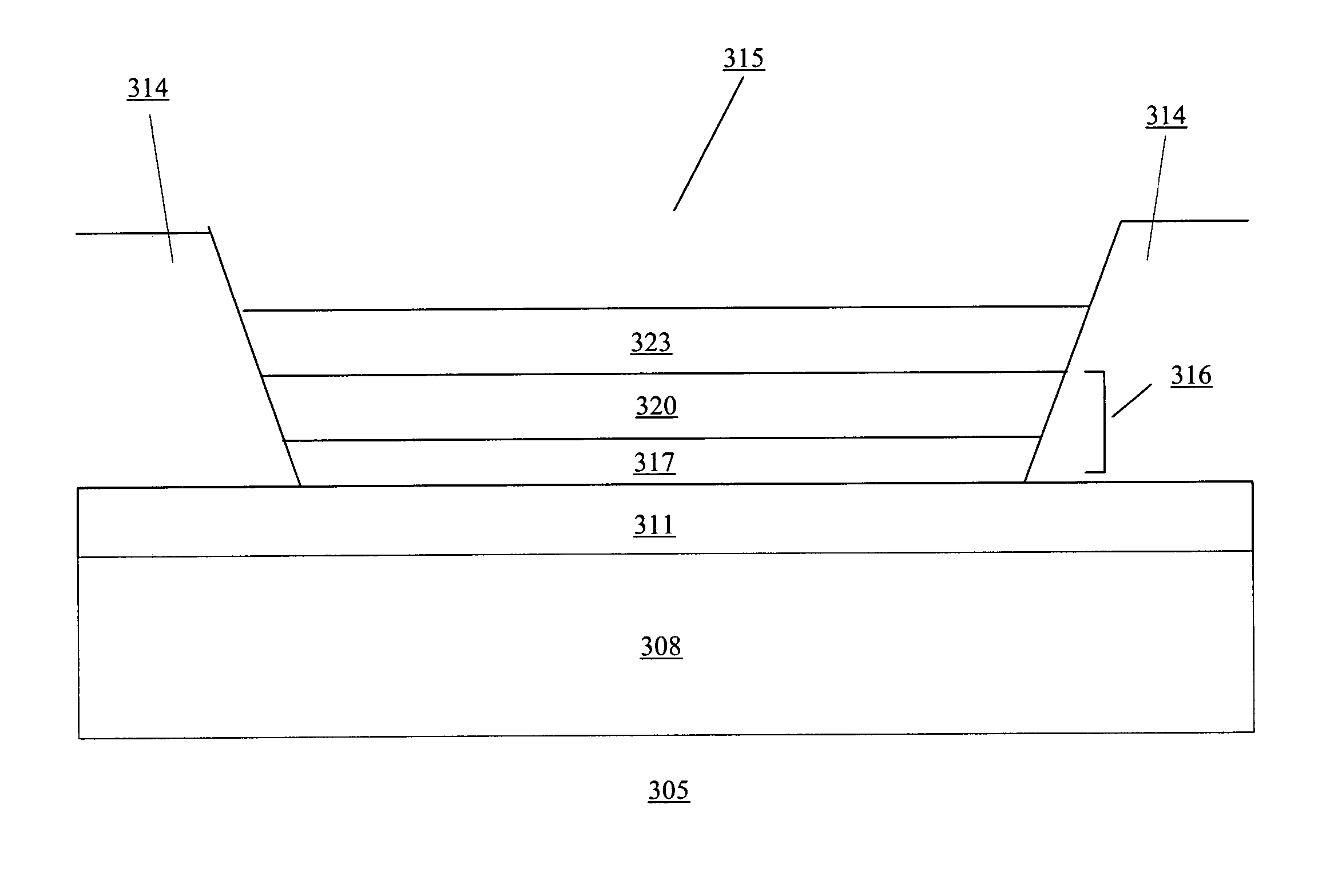
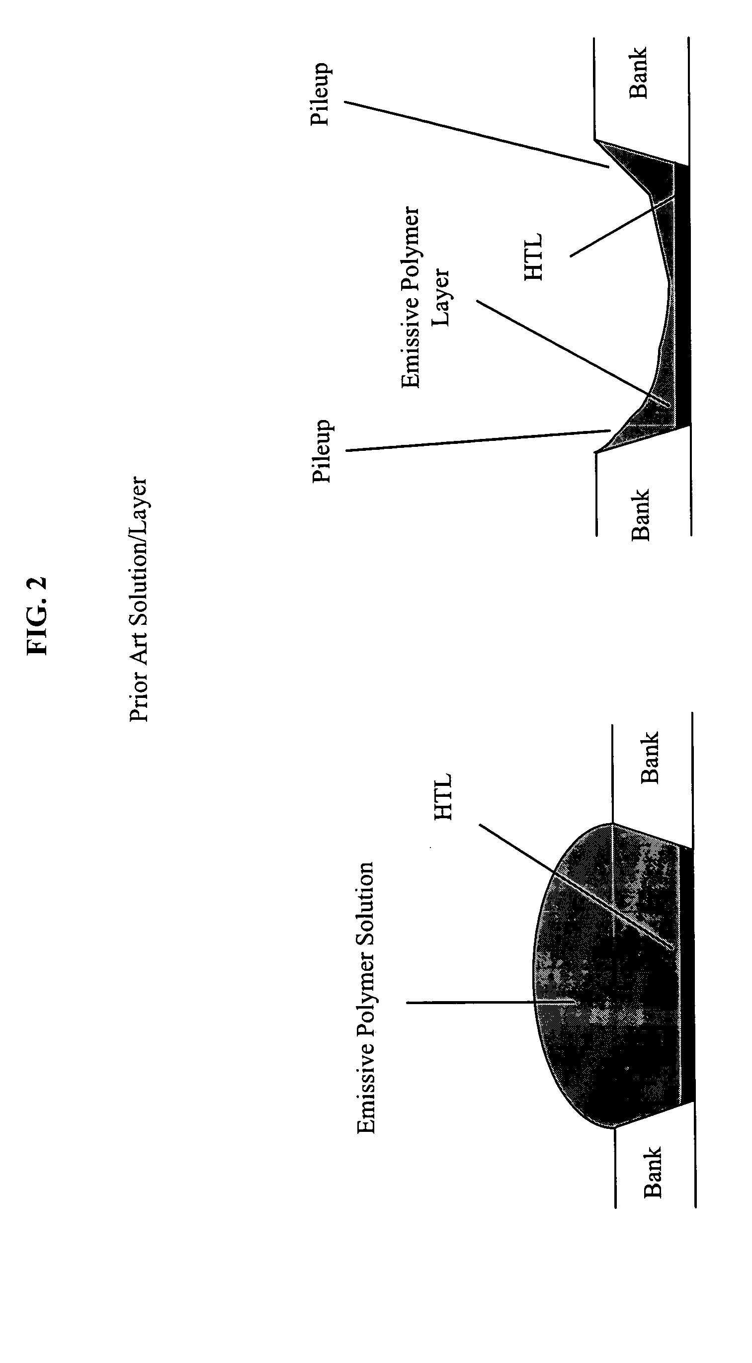
[0016] The one or more solvents used to dissolve the organic polymers are one of the important factors determining the uniformity or flatness of the resulting dried layer. The uniformity of the resulting layer can be controlled by the solvents used to dissolve the organic polymers. An organic polymer solution is made by mixing together at least one organic polymer and a first solvent, and then adding a second solvent to the mixture. Alternatively, the solution can be made by mixing the first solvent and the second solvent and then adding the one or more polymers to the mixture. The first solvent has a high solubility (e.g., the first solvent dissolves at least about one weight percent of the organic polymers) and a faster evaporation rate than the second solvent, and the second solvent has a very low solubility (e.g., the second solvent dissolves less than about one-fourth weight percent of the organic polymers). The first solvent can have a lower boiling point than the second solve...
PUM
 Abstract
Description
Claims
Application Information