Method and system for treating a dielectric film

a dielectric film and treatment method technology, applied in the direction of electrical equipment, semiconductor devices, semiconductor/solid-state device details, etc., can solve the problems of poor adhesion of the barrier layer to the dielectric film, the interconnection delay is a major limitation factor, and the film is less robust than the more traditional dielectric layer,

a dielectric film and treatment method technology, applied in the direction of electrical equipment, semiconductor devices, semiconductor/solid-state device details, etc., can solve the problems of poor adhesion of the barrier layer to the dielectric film, the interconnection delay is a major limitation factor, and the film is less robust than the more traditional dielectric layer,

US20050077597A1Inactive Publication Date: 2005-04-14TOKYO ELECTRON LTD

Image

  • Method and system for treating a dielectric film
  • Method and system for treating a dielectric film
  • Method and system for treating a dielectric film

Examples


Embodiment Construction

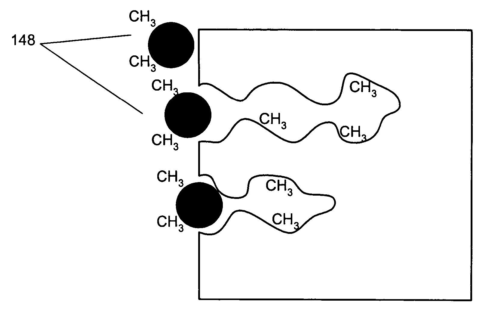
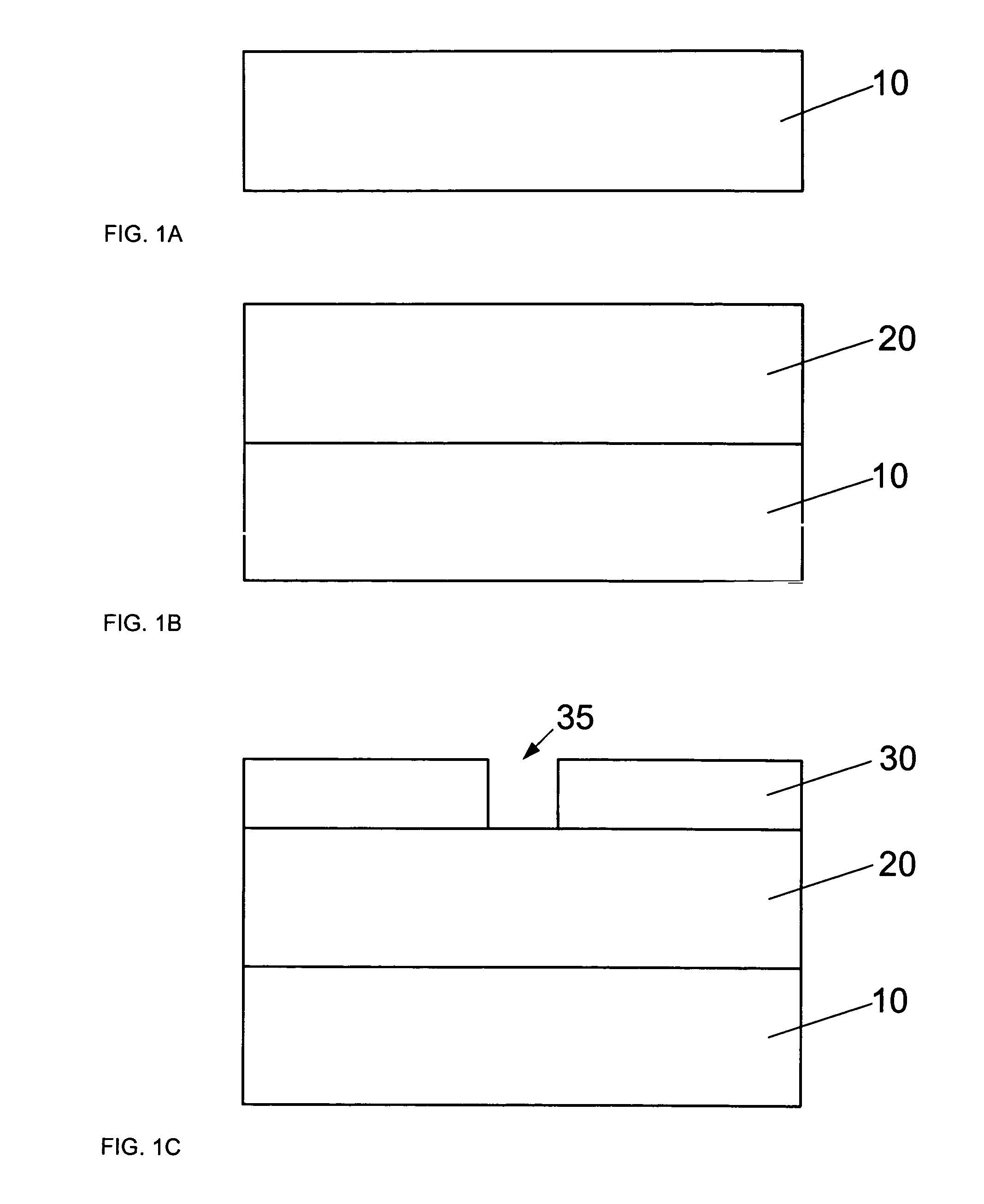
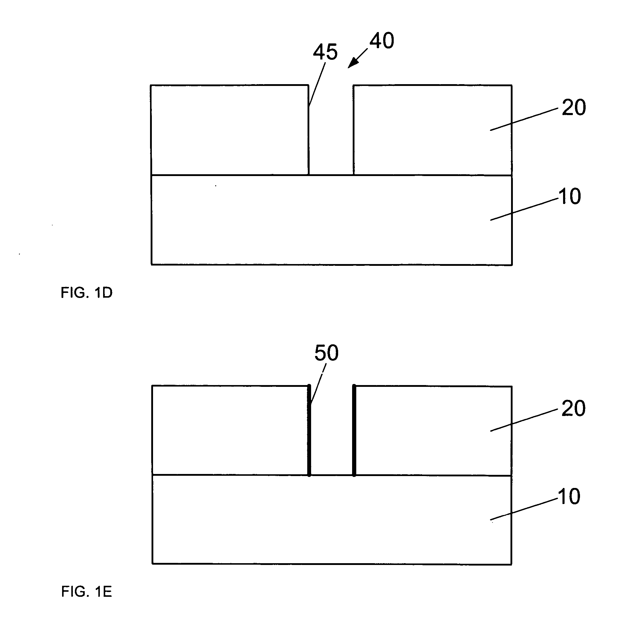
[0031] Referring now to the drawings, wherein like reference numerals designate identical or corresponding parts throughout the several views, FIGS. 1A through 1E present a schematic representation of a method of forming a pattern in a dielectric film and treating the exposed surfaces of the etched pattern in the dielectric film in order to perform at least one of healing, sealing, and cleaning these surfaces. Additionally, FIG. 2 presents a flow chart 100 of performing the method according to an embodiment of the present invention. As shown in FIGS. 1A, 1B, and 2, a dielectric film 20 is formed in 110 on an upper surface of a substrate 10 that may or may not include additional layers. The substrate 10 may be a semiconductor, a metallic conductor, or any other substrate to which the dielectric film is to be formed upon. The dielectric film has a nominal dielectric constant value less than the dielectric constant of SiO2, which is approximately 4 (e.g., the dielectric constant for th...


PUM


Abstract

A method and system for treating a dielectric film includes exposing at least one surface of the dielectric film to a CxHy containing material, wherein x and y are each integers greater than or equal to a value of unity. The dielectric film can include a low dielectric constant film with or without pores having an etch feature formed therein following dry etch processing. As a result of the etch processing or ashing, exposed surfaces in the feature formed in the dielectric film can become damaged, or activated, leading to retention of contaminants, absorption of moisture, increase in dielectric constant, etc. Damaged surfaces, such as these, are treated by performing at least one of healing these surfaces to, for example, restore the dielectric constant (i.e., decrease the dielectric constant) and cleaning these surfaces to remove contaminants, moisture, or residue. Moreover, preparation for barrier layer and metallization of features in the film may include treating by performing sealing of sidewall surfaces of the feature to close exposed pores and provide a surface for barrier film deposition.

Description

BACKGROUND OF THE INVENTION [0001] 1. Field of the Invention [0002] The present invention relates to a method and system for treating a dielectric film and, more particularly, to a method and system of treating a dielectric film in order to perform at least one of healing, sealing, and cleaning the dielectric film. [0003] 2. Description of Related Art [0004] [0002]As is known to those in the semiconductor art, interconnect delay is a major limiting factor in the drive to improve the speed and performance of integrated circuits (IC). One way to minimize interconnect delay is to reduce interconnect capacitance by using low dielectric constant (low-k) materials during production of the IC. Such low-k materials have also proven useful for low temperature processing. Thus, in recent years, low-k materials have been developed to replace relatively high dielectric constant insulating materials, such as silicon dioxide. In particular, low-k films are being utilized for inter-level and intra...

Claims


Application Information

Patent Timeline
14 Apr 2005
Publication
US20050077597A1
IPC
H01L21/311; H01L21/316; H01L21/768; H01L23/532
CPC
H01L21/02063; H01L21/3105; H01L21/31058; H01L21/31138; H01L21/76826; H01L21/02359; H01L23/5329; H01L21/02126
Inventors
TOMA, DOREL IOAN; ZHU, JIANHONG