Field emission device and method of fabricating same

Inactive Publication Date: 2005-04-14
NANYANG TECH UNIV
View PDF4 Cites 7 Cited by
  • Summary
  • Abstract
  • Description
  • Claims
  • Application Information

AI Technical Summary

Benefits of technology

[0005] The present invention was developed with a view to providing a field emission component for a field emission device with a relatively large and thermally stable emission area, and a simple method of fabricating same.
[0016] a metal-carbon composite film deposited on a suitable substrate, said film having been thermally treated post-deposition to form nano-particles and / or nanotubes therein whereby, in use, said field emission component has a relatively large surface area and improved emission spot density.

Problems solved by technology

Although they produce high-quality displays, system costs are high and production yields are very poor.
This is because they are working at the limits of photofabrication with slow and expensive step and repeat exposures.
It is very difficult to scale up this approach to large area displays.
However, high temperature deposition with low growth rate and small area for the diamond film, limits diamond films for practical application.
Although diamond-like carbon films can be deposited with a high rate at low temperature over a large area, the field emission properties are poor.
Conditioning phenomena (pretreating the film surface by using a high voltage) exists in the emission process for diamond and DLC films, which occurs randomly and is difficult to control.
However, controllability of CNT film is difficult and the adhesion between CNT film and substrate is poor by using normal chemical vapour deposition method.

Method used


Image

  • Field emission device and method of fabricating same
  • Field emission device and method of fabricating same
  • Field emission device and method of fabricating same

Examples


example 1

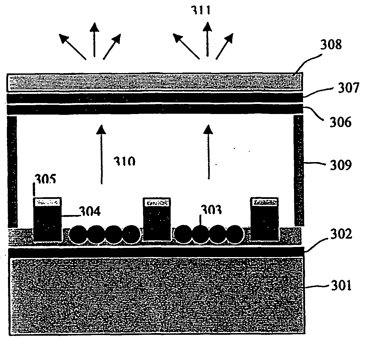
[0039] The emission current density dependence on the applied field for a FeC composite film prepared by using this invention is shown in FIG. 6. An image of the spatial emission spots on the ITO-glass anode is inserted in the drawing. The emission area is 6 mm in diameter. Clearly, the FeC film shows a very good emission property, i.e., high emission current density (10 mA / cm2 at 10 V / μm), low turn-on emission field (1 V / μm at 1 nA / cm2), high emission spot density (104 / cm2), and a uniform distribution of spatial emission spots.

example 2

[0040] FIGS. 7(a) and (b) show examples of diode-type field emission displays using a carbon composite film as emitter. A star image about 5 mm in size on a ZnO:Zn phosphor coated ITO plate can been seen in FIG. 7(a), with an applied field of 10 V / μm. A uniform emission image with high emission spots has been obtained at such low field. FIG. 7(b) shows a line image of field emission array on ITO plate. The line width is 100 μm, the applied field is 12 V / μm. Twelve pieces of luminance lines of 10 mm in length can be clearly seen. From this result, it is apparent that a high-resolution field emission display can be achieved using the invented carbon composite films as emitters.

[0041] Now that preferred embodiments of the field emission component for a field emission device (FED) and method of fabricating same have been described in detail, it will be apparent that they provide a number of significant advantages over comparable prior art techniques, including, but not limited, to the ...


PUM

PropertyMeasurementUnit
Temperatureaaaaaaaaaa

Abstract

This invention relates to a method of fabricating a field emission device (FED) by using a carbon composite film, the composite film providing a field emission layer which consists of fine carbon-metal grains and / or carbon nanotubes, so that (a) a threshold voltage required for emitting electrons from the field emission device can be lowered significantly; (b) a stable electron beam of the field emission display device can be increased; and, (c) emission Uniformity and emission spot density can be greatly improved. The fabrication method involves preparing a metal-carbon composite film on a suitable substrate using an appropriate deposition technique. The carbon composite film is then thermally treated post-deposition, so as to form nano-particles and / or nanotubes in the film. Post-treatment of the composite film may involve annealing or plasma etching using hydrogen or hydrocarbon gas to reduce the electron emission barrier. During deposition of the metal-carbon composite film, the composition of the metal content in the film can be tuned to control the field emission properties of the field emission component.

Description

FIELD OF THE INVENTION [0001] The present invention relates to a field emission device (FED) and method of fabricating same and relates particularly, though not exclusively, to a method of fabricating a field emission component for use in flat panel displays and vacuum microelectronics applications. BACKGROUND TO THE INVENTION [0002] A field emission cathode has been used in flat panel displays and vacuum microelectronics applications. Cold cathode and field emission based flat panel displays have several advantages over other types of flat panel displays. These include low power dissipation, high intensity and low projected cost. Conventionally, to fabricate a sub-micron stiff silicon or molybdenum tips, a complicated micro-fabrication technique for preparation of three dimensional structures by a repeated process of depositing and etching has been used. Present small FED cathodes use arrays of microtips with gate apertures of about 1 μm in diameter. These are made in a semiconduct...

Claims


Application Information

Patent Timeline
IPC IPC(8): C23C14/06C23C14/58C23C16/30C23C16/56H01J9/02
CPCB82Y10/00B82Y30/00C23C14/06H01J9/025C23C16/30C23C16/56C23C14/58
Inventor SUN, ZHUOTAY, BENG KANGLAU, SHU PINGLI, YUNJUN
Owner NANYANG TECH UNIV
Why Eureka
Try Eureka