Near-field exposure photoresist and fine pattern forming method using the same
- Summary
- Abstract
- Description
- Claims
- Application Information
AI Technical Summary
Benefits of technology
Problems solved by technology
Method used
Image

Examples
example
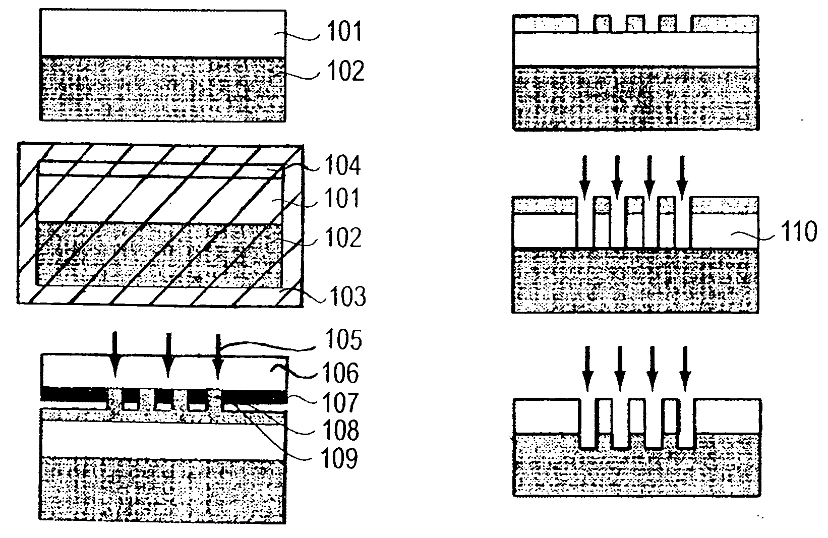
[0071] In order to form a 50 nm L / S (line and space) pattern of a 100 nm-thick upper Si layer on SiO2 layer of SOI (silicon on insulator) substrate, a photoresist was formed on the SOI substrate by spin coating.
[0072] The photoresist contained an alkali-soluble novalac resin, a photosensitizer having a naphthoquinonediazyde group, triazine and a sensitizer.
[0073] With respect to the thickness of the photoresist layer, it is necessary to provide the photoresist layer on the SOI substrate with a thickness of to less than 50 nm in view of a ratio of etching resistance between Si and the photoresist with respect to a mixture gas of CHF3 and SF6 since Si is etched with the mixture gas. Further, in order to form the 50 nm L / S pattern by near-field exposure, a width of a small opening of the photomask used in the near-field exposure is approximately 20 nm. For this reason, a thickness of the silylation portion is determined as 20 nm.
[0074] When a 20 nm-thick silylation portion is used a...
PUM
 Abstract
Description
Claims
Application Information
 - R&D Engineer
- R&D Manager
- IP Professional
- Industry Leading Data Capabilities
- Powerful AI technology
- Patent DNA Extraction
Browse by: Latest US Patents, China's latest patents, Technical Efficacy Thesaurus, Application Domain, Technology Topic.
© 2024 PatSnap. All rights reserved.Legal|Privacy policy|Modern Slavery Act Transparency Statement|Sitemap