Ceramic package and chip resistor, and method for manufacture thereof

a technology of ceramic packaging and chip resistor, which is applied in the direction of resistor chip manufacture, resistor details, semiconductor/solid-state device details, etc., can solve the problems of high cost, poor work efficiency, and poor work efficiency, and achieve the effect of increasing cos

Inactive Publication Date: 2005-04-21
NIPPON CARBIDE KOGYO KK
View PDF2 Cites 20 Cited by
  • Summary
  • Abstract
  • Description
  • Claims
  • Application Information

AI Technical Summary

Benefits of technology

[0006] Accordingly, the objects of the present invention are to solve the problems in the work efficiency of the product

Problems solved by technology

Recently, when production of ceramic packages having a size of 4 mm square or less is required, there has been the problem that the work efficiency has been extremely poor and the cost becomes high.
Further, the formation of a conductor layer on a package with step differences has the problem of requiring individual packages to be processed, and therefore, the work efficiency is an extremely poor.
Note that, in the powder pressing method of the prior art as well, sometimes a large number of packages are handled, but due to the brittleness, when handling thin sheets, a sheet size of about 1 inch square is the limit and the work efficiency is poor.
The lamination method of the prior art laminates sheets, and therefore, the work efficiency would appear, at first glance, to be good, but since it is necessary to punch holes in, print on, and form conductor layers on the individual green sheets and laminat

Method used


Image

  • Ceramic package and chip resistor, and method for manufacture thereof
  • Ceramic package and chip resistor, and method for manufacture thereof
  • Ceramic package and chip resistor, and method for manufacture thereof

Examples


example 1

[0062] (1) Production of Plastic Ceramic Green Sheet Slurry

[0063] As the ceramic powder, 100 parts by weight of alumina filler-containing borosilicate glass (made by Nihon Yamamura Glass: BS-003; alumina to borosilicate glass (weight ratio)=50:50), 20 parts by weight of an ethyl acrylate / methyl methacrylate / 2-hydroxyethyl methacrylate copolymer (weight ratio: 85 / 12 / 3, Tg=−15° C., weight average molecular weight (MW) converted to polystyrene 500,000) as an acryl binder, 4 parts by weight of di(2-ethylhexyl) phthalate and 1 part by weight of a butylbenzyl phthalate as plasticizers, and 55 parts by weight of a solvent (toluene / methylisobutylketone / n-butanol=1 / 1 / 1 (weight ratio)) were mixed by a dispersion mixer so as to obtain a ceramic green sheet slurry having a viscosity of 18,000 cps.

[0064] (2) Production of Plastic Ceramic Green Sheet

[0065] The above ceramic green sheet slurry was coated on a support film (weight 400 mm, length 100 m, thickness 100 μm) composed of polyethylene ...

example 2

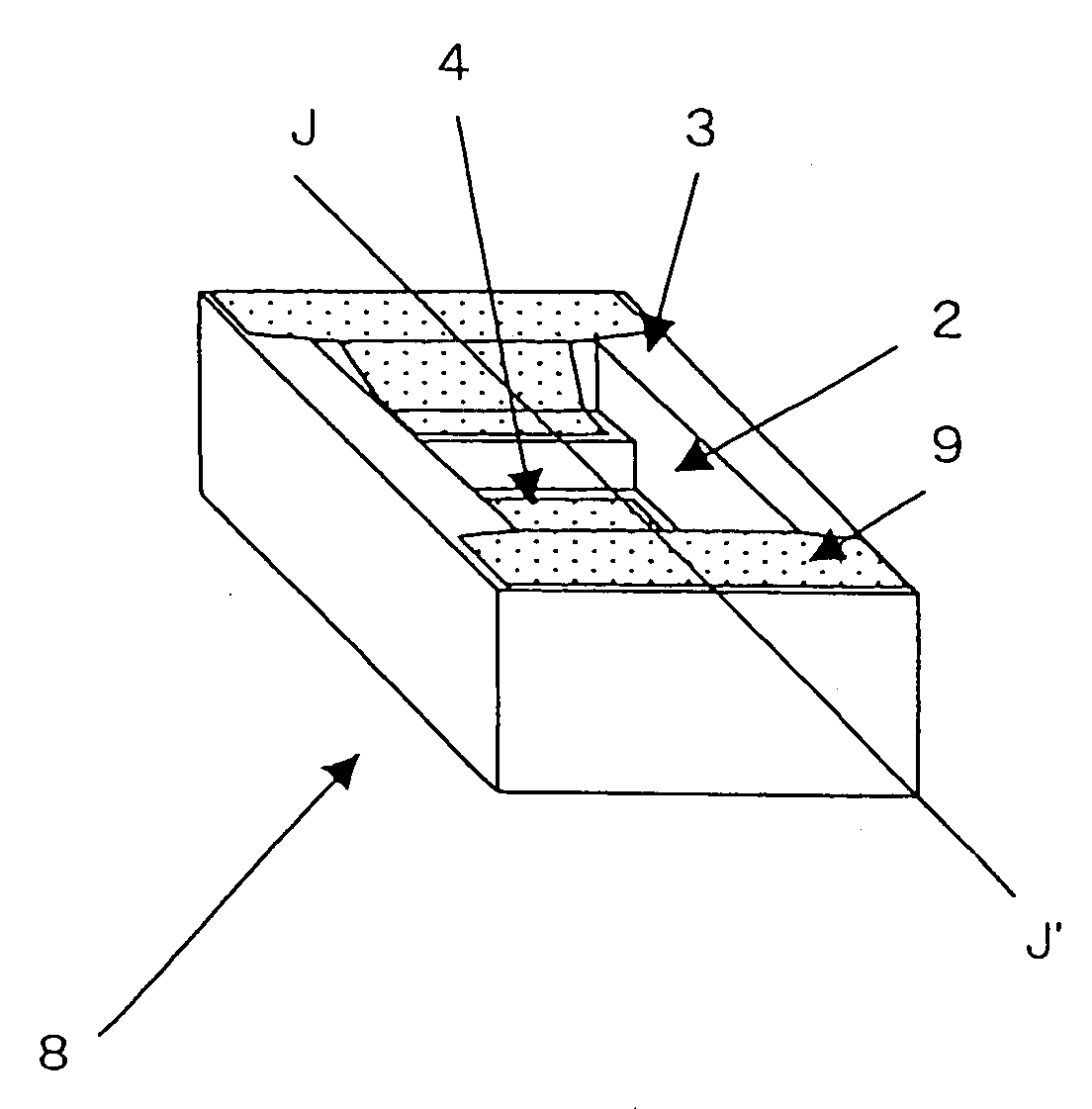
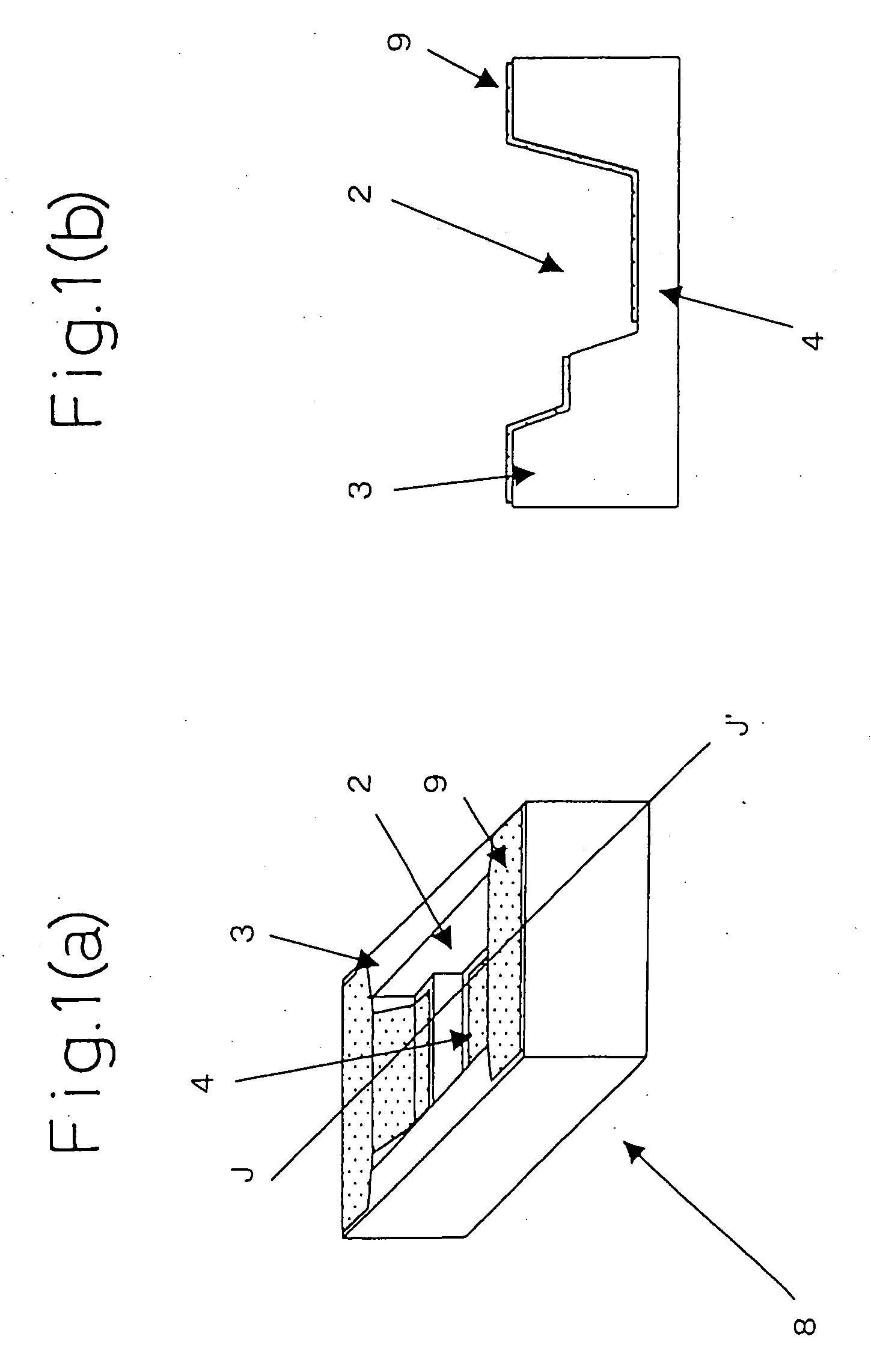
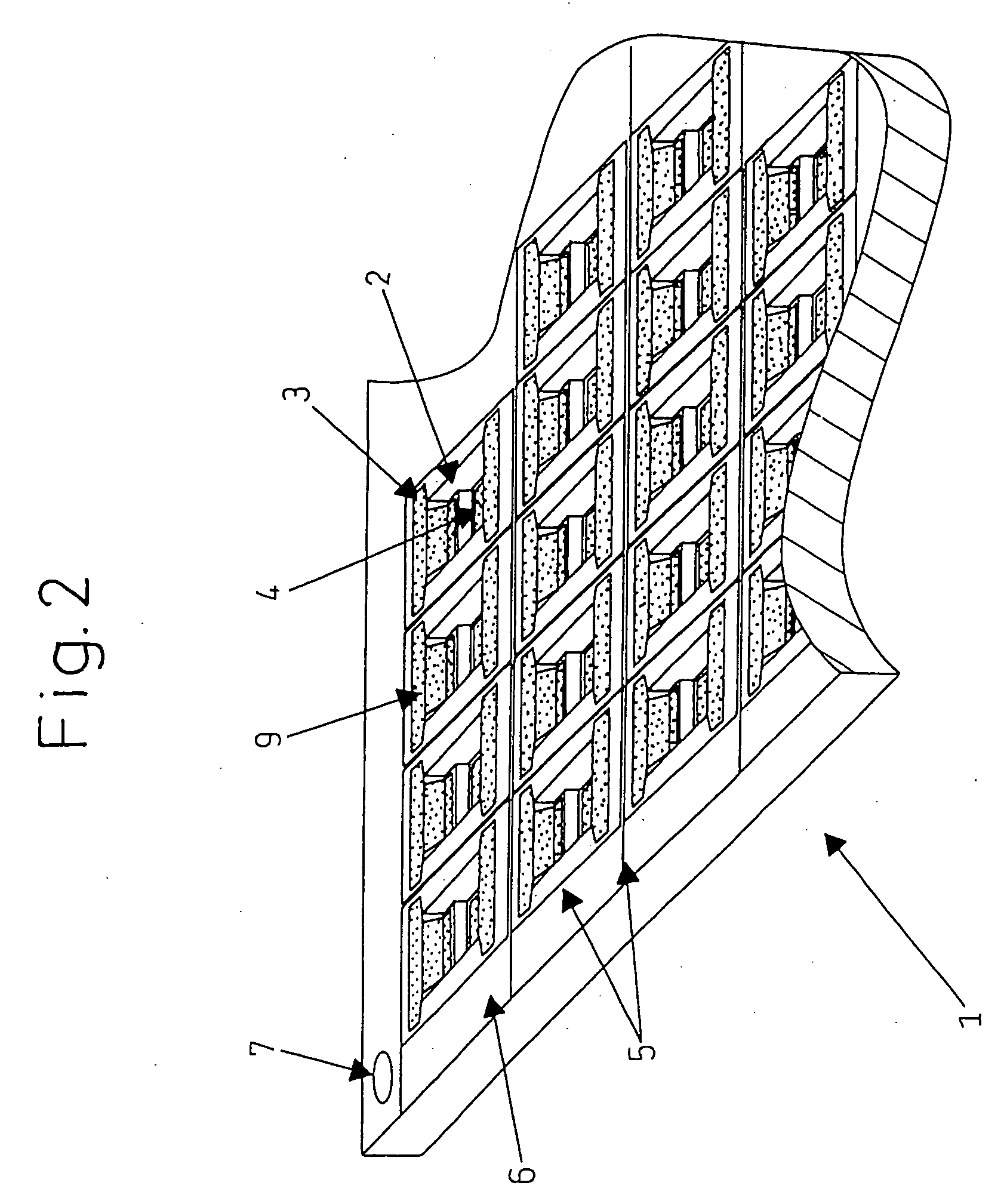
[0079] The same procedure was followed as in Example 1 to produce a ceramic green sheet, form a conductor layer 9, form a plurality of recesses by press forming in a regular order, without forming break grooves 5, as in FIG. 2, and calcine the ceramic green sheet to produce a ceramic cell sheet 10 composed of a plurality of ceramic cell units (i.e., ceramic package in broad sense such as plasma display panel having plurality of recesses arranged in regular order) (see FIG. 3).

example 3

[0080] Except for making the acrylic binder used in Example 1, 20 parts by weight of a lauryl methacrylate / isobutyl methacrylate / 2-hydroxyethyl methacrylate copolymer (weight ratio 60 / 37 / 3, Tg=−15° C., MW 350,000), the same procedure was followed as in Example 1 to produce a green sheet slurry. The slurry thus obtained was coated by a comma roll coater in the same way as in Example 1 to obtain a 700 μm ceramic green sheet. The ceramic green sheet thus obtained was pressed in a mold and the shape observed. Compared with Example 1, the transfer of the projecting shapes of the mold was somewhat inferior, but this was out of a level posing a problem in function.


PUM

PropertyMeasurementUnit
Temperatureaaaaaaaaaa

Abstract

A ceramic package and a chip resistor obtained by forming, on a plastic ceramic green sheet comprising 100 parts by weight of a ceramic powder mainly composed of borosilicate glass, into which 10 to 30 parts by weight of an acrylic copolymer obtained by polymerizing 100 parts by weight of a (meth)acrylic acid ester and 1 to 10 parts by weight of a monomer having a functional group of a hydroxyl group, acid amide group, or amino group and having a Tg in the range of −30° C. to +10° C. is compounded, a conductor layer using a plastic conductive paste obtained by compounding, into 100 parts by weight of a conductive powder, 5 to 20 parts a mixture of an acrylic copolymer having a Tg of not more than −30° C. and an ethylcellulose-based binder, press forming the resultant single layer of ceramic green sheet, and calcining the resultant ceramic green sheet having the integrally formed bottom, opening and opening circumferential edge and a method for producing the same.

Description

TECHNICAL FIELD [0001] The present invention relates to a ceramic package for storing a device for an electronic component, a chip-type resistor and methods for the production of the same. BACKGROUND ART [0002] A ceramic package for storing a device for an electronic component formed with a bottom, an opening, and an opening circumferential edge has been proposed and put into use. As a typical method for production of a conventional ceramic package, the method of pressing a ceramic powder composed of a powder of a ceramic, to which a binder has been added, in a mold having a desired shape, sintering the press formed body, then forming a conductor layer after the sintering is known (for example, see Japanese Unexamined Patent Publication (Kokai) No. 2001-181023). As another conventional method of production of a ceramic package, a lamination method of pressing and heating a plurality of ceramic green sheets formed with holes, printed on, and formed with conductor layers so as to lami...

Claims


Application Information

Patent Timeline
IPC IPC(8): C03C14/00C04B35/634H01C1/028H01C17/00H01C17/02H01C17/065H01L21/48H05K1/00H05K1/03H05K1/09H05K3/00
CPCC03C14/004H05K2203/0108C03C2214/12C03C2214/20C03C2214/30C04B35/62625C04B35/6263C04B35/6264C04B35/63424C04B2235/602H01C1/028H01C17/006H01C17/02H01C17/06533H01C17/06593H01L21/4807H05K1/0284H05K1/0306H05K1/092H05K3/0014C03C2214/04
Inventor NAITO, JUNYAISHITA, FUMIOSHIBATA, ATSUSHIYAMAGATA, NOBORU
Owner NIPPON CARBIDE KOGYO KK
Why Eureka
Try Eureka