Timing recovery circuit and timing recovery method

a timing recovery and circuit technology, applied in the direction of pulse manipulation, pulse technique, baseband system details, etc., can solve the problems of signal arriving at a receiver by different paths showing different time delays, inter-symbol interference (isi), degradation of reception

Active Publication Date: 2005-04-21
SAMSUNG ELECTRONICS CO LTD
View PDF6 Cites 19 Cited by
  • Summary
  • Abstract
  • Description
  • Claims
  • Application Information

AI Technical Summary

Benefits of technology

[0025] An exemplary embodiment of the present invention is directed to a timing recovery circuit for a receiver. The timing recovery circuit may include a timing error detector that generates a timing error based on differences between coefficients of a feed-forward filter and a feed-back filter. The timing recovery circuit may also include a loop filter which generates a control voltage signal based on the timing error, and a voltage controlled that generates a sampling clock for the receiver based on the generated control voltage signal.
[0026] Another exemplary embodiment of the present invention is directed to a method of recovering symbol-rate timing for a receiver having a decision feedback equalizer that includes a feed-forward filter and a feed-back filter. A timing error may be generated as a function of a first difference between a dominant precursor tap coefficient value of the feed-forward filter and a center tap coefficient value of the feed-back filter. The timing error may be revised by generating a first modified timing error as a function of a second difference between a first initial coefficient value and a converging value of the dominant precursor tap coefficient of the feed-forward filter. The first modified timing error may be revised by generating a second modified timing error as a function of a third difference between a second initial coefficient value and a converging value of the center tap coefficient of the feed-back filter. The second modified timing error may be output to generate a control voltage signal for controlling a sampling clock of the receiver for sampling a received signal.

Problems solved by technology

In some wireless or high-speed data communication systems, signals arriving at a receiver by different paths show different time delays.
This results in inter-symbol interference (ISI), a degradation in reception.
Amplitude and phase of a received signal may be severely distorted, and may cause a bit error in the receiver.
This kind of channel characteristic results in the dispersion of an impulse, sent by the transmitter, at the receiver, thus corrupting the reception.
This dispersion is referred to as ISI, and results in data loss and hence, loss of communication reliability.
High-frequency loss in the channel tends to reduce the slope of the pulse edges resulting in finite rise times, known as ‘precursor distortion’.
At low frequencies, the nonlinear phase characteristics tend to produce a substantially long decay tail, or ‘postcursor distortion’, resulting in a smeared pulse shape.
Distortion suffered by a given pulse results in interference to its neighbors in time.
Thus, at the receiver, detection of symbols is further complicated by the presence of pulse distortion in addition to noise.
In addition, timing errors increase for the severely distorted channel, according to the M&M algorithm.
This process requires an exact control of a loop filter, however, since either the precursor or the timing error is distorted based on the channel status.
Thus, extracting timing information by the cross-correlating precursor and timing error process requires substantial hardware.
However, the converging properties of the coefficients of the DFE may be greatly affected by the initial phase of a PLL, in the case a PLL is used to extract timing information.
Accordingly, the converging property of the DFE may be inadequate, depending on the initial phase of timing recovery; thus the prior art method of FIG. 1 requires a control block for controlling the initial phase, as described by the M&M algorithm.
Therefore, large timing errors may occur for unknown channels or for properties of a channel that vary over time.

Method used


Image

  • Timing recovery circuit and timing recovery method
  • Timing recovery circuit and timing recovery method
  • Timing recovery circuit and timing recovery method

Examples


Embodiment Construction

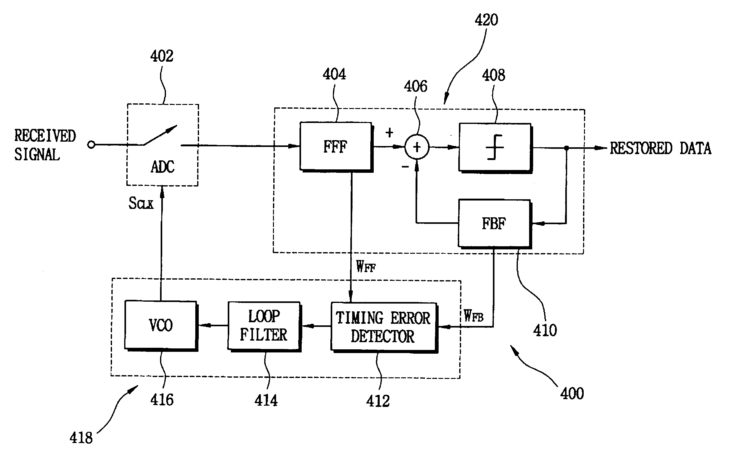
[0036]FIG. 4 is a block diagram illustrating a timing recovery system according to an exemplary embodiment of the present invention. Referring to FIG. 4, system 400 may be implemented within a symbol-rate receiver, for example, and may include an analog-to-digital converter (ADC) 402, a decision feedback equalizer (DFE) 420 and a timing recovery circuit 418. The timing recovery circuit 418 may include a timing error detector 412, a loop filter 414 and a voltage controlled oscillator (VCO) 416. Timing error detector 412, loop filter 414 and VCO 416 together may form a Phase-Locked Loop (PLL). A feed-forward filter (FFF) 404 and a feedback filter (FBF) 410 are included in DFE 420 in an effort to reduce pre-cursors and post-cursors of the channel impulse response, respectively.

[0037] Referring to FIG. 4, the ADC 402 samples a received signal (which may be a continuous-time signal for example) using a sampling clock (SCLK) and converts the continuous-time signal to a discrete-time sign...


PUM


Abstract

A timing recovery circuit for a receiver may include a timing error detector that generates a timing error based on differences between coefficients of a feed-forward filter and a feed-back filter. The timing recovery circuit may include a loop filter which generates a control voltage signal based on the timing error, and a voltage controlled oscillator that generates a sampling clock for the receiver based on the generated control voltage signal.

Description

CROSS-REFERENCE TO RELATED APPLICATIONS [0001] This U.S. nonprovisional patent application claims priority under 35 U.S.C. § 119 of Korean Patent Application No. 2003-56400, filed on Aug. 14, 2003, the entire contents of which are hereby incorporated by reference.BACKGROUND OF THE INVENTION [0002] 1. Field of the Invention [0003] The present invention relates to a timing recovery circuit and a timing recovery method. [0004] 2. Description of the Related Art [0005] In some wireless or high-speed data communication systems, signals arriving at a receiver by different paths show different time delays. This results in inter-symbol interference (ISI), a degradation in reception. Amplitude and phase of a received signal may be severely distorted, and may cause a bit error in the receiver. [0006] For example, one high-speed data communication system where this is of concern is in systems employing Digital Subscriber Line (DSL) technology. DSL, which provides high-speed communications using...

Claims


Application Information

Patent Timeline
Patent Type & Authority Applications(United States)
IPC IPC(8): H04L27/00H04L7/02H04L25/03
CPCH04L25/03057H04L7/0058H04L27/00
Inventor SEO, IL-WON
Owner SAMSUNG ELECTRONICS CO LTD
Why Eureka
Try Eureka