Control of carbon nanotube diameter using CVD or PECVD growth

a carbon nanotube and diameter technology, applied in the field of carbon nanotube diameter control, can solve the problems of catalyst agglomeration, complicated and difficult control of synthesis of small catalyst particles with a narrow diameter distribution, and limit the usefulness of this technique for circuit applications

a carbon nanotube and diameter technology, applied in the field of carbon nanotube diameter control, can solve the problems of catalyst agglomeration, complicated and difficult control of synthesis of small catalyst particles with a narrow diameter distribution, and limit the usefulness of this technique for circuit applications

US20050089467A1Active Publication Date: 2005-04-28GLOBALFOUNDRIES US INC

Image

  • Control of carbon nanotube diameter using CVD or PECVD growth
  • Control of carbon nanotube diameter using CVD or PECVD growth
  • Control of carbon nanotube diameter using CVD or PECVD growth

Examples


example 2

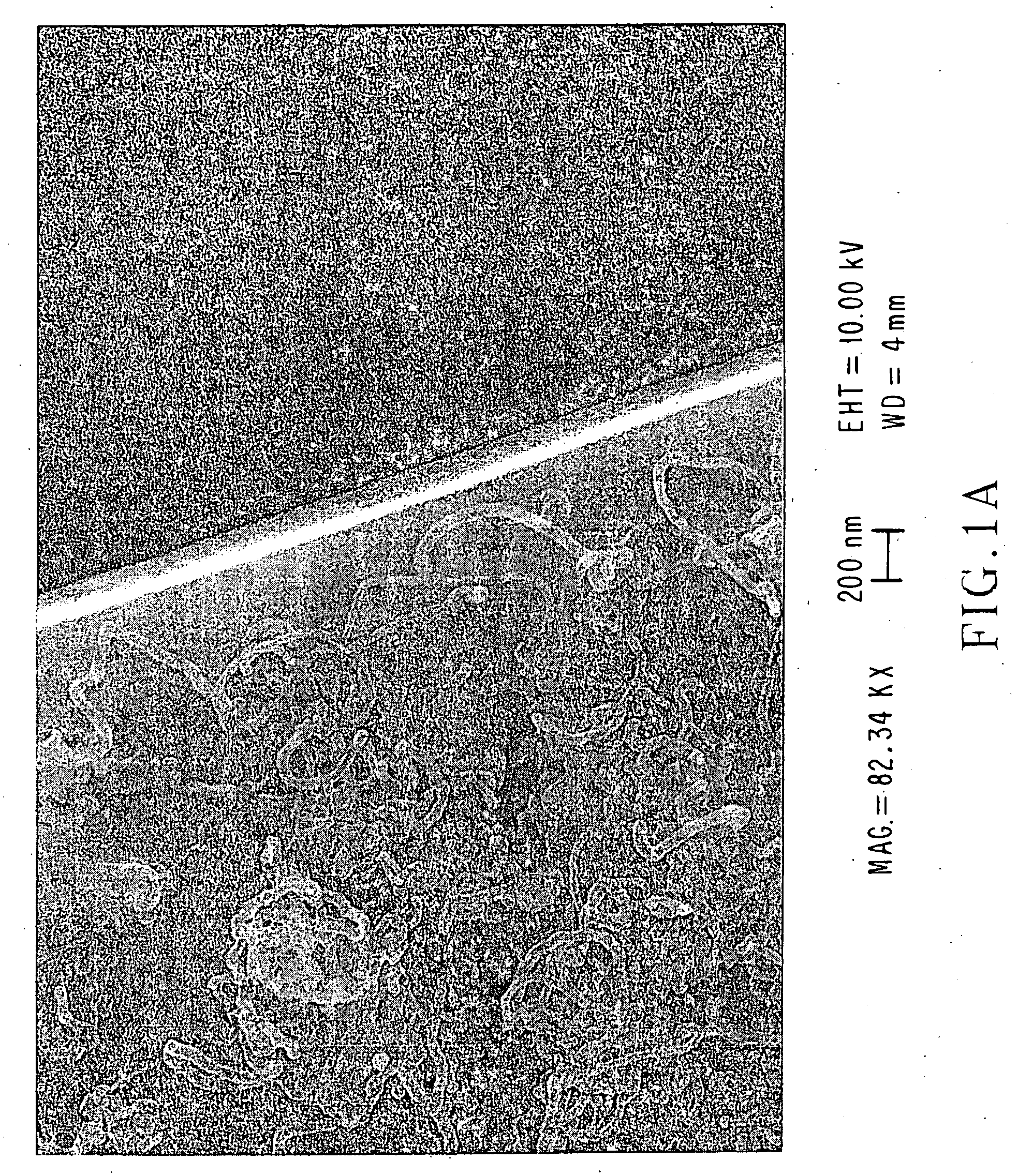
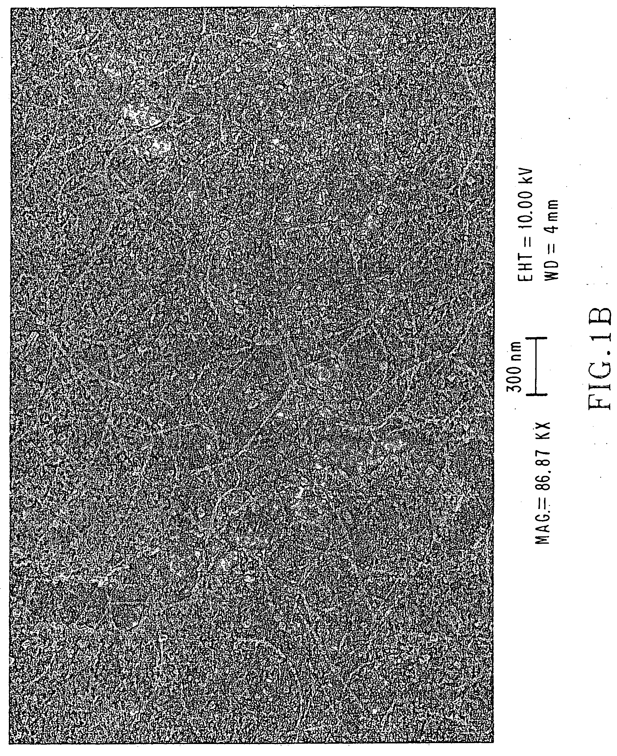
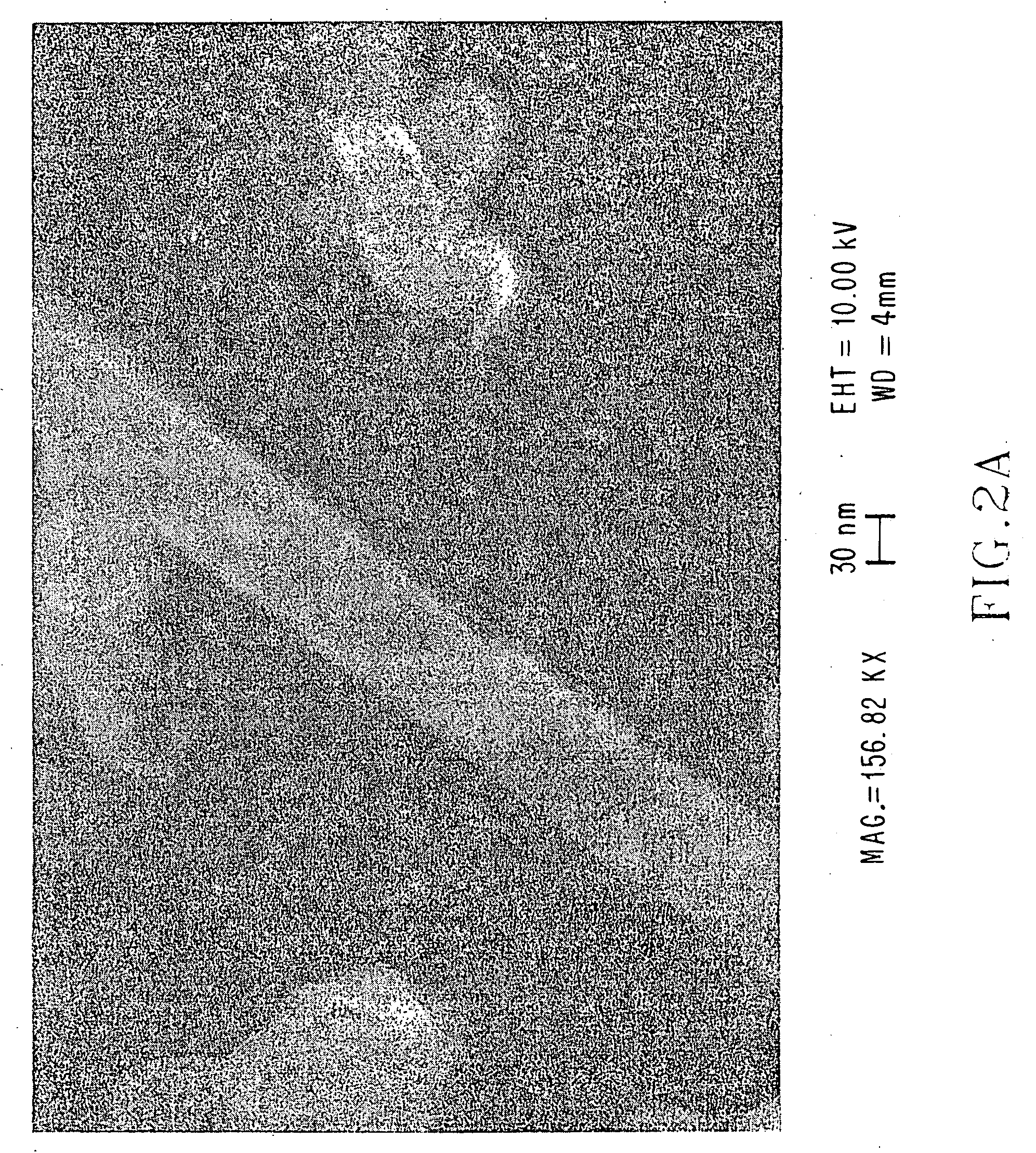
[0054] This example demonstrates the effects of growth pressure on CNT diameter. A catalyst comprising a 2 nanometers thick patterned film of Fe is heated up to the growth temperature of 950° C. in a hydrogen gas ambient. FIGS. 2(a)-2(b) illustrate the effects of growth pressure on CNT diameter. FIG. 2(a) shows a scanning electron micrograph of CNTs grown at 80 torr and methane flow of 100 sccm (tr-6 min), while FIG. 2(b) shows an atomic force microscopy image of CNTs grown at 40 torr for the same methane flow rate (tr-3 min). It is evident that the lower growth pressure results in CNTs with a much smaller diameter. While the dCNT=2.5±1.5 nanometers for the growth at 40 torr, the CNT diameter is much larger (on the order of 50 nanometers) for a growth pressure of 80 torr.

[0055] From the above it is clear that the residence time can be used to control tube diameter from b).

[0056] The carbon nanotubes according to the present invention can be used in fully integrated structures usin...


PUM

PropertyMeasurementUnit
Temperatureaaaaaaaaaa
Diameteraaaaaaaaaa
Diameteraaaaaaaaaa

Abstract

The diameter of carbon nanotubes grown by chemical vapor deposition is controlled independent of the catalyst size by controlling the residence time of reactive gases in the reactor.

Description

TECHNICAL FIELD [0001] The present invention relates to carbon nanotube growth using chemical vapor deposition (CVD) or plasma enhanced chemical vapor deposition (PECVD), and more specifically to the control of the carbon nanotube diameter during the CVD or PECVD growth. BACKGROUND ART [0002] Carbon nanotube based field effect transistors (CNTFETs) show great promise for device applications. Recently CNTFETs with excellent electrical characteristics comparable to state-of-the-art silicon MOSFETs have been demonstrated [see, for example, Rosenblatt et al., “High Performance Electrolyte-Gates Carbon Nanotube Transistors”, NanoLetters, 2(8), (2002) pp. 869-72]. The electrical characteristics of CNTFETs however depends largely on the band-gap of the single wall carbon nanotube (SWNT) forming the channel of the transistor. Since the band-gap of SWNTs has a strong dependence on the diameter, accurate control of the diameter is essential to the success of any device technology based on car...

Claims


Application Information

Patent Timeline
28 Apr 2005
Publication
US20050089467A1
IPC
C01B31/02; C23C16/26; C23C16/52; C30B25/00; C30B25/10; C30B29/60; D01F9/12; H01J9/02; H01L51/30; H05H1/24
CPC
B82Y10/00; B82Y30/00; B82Y40/00; C01B31/0233; C01B2202/36; Y10S977/843; C30B25/105; C30B29/605
Inventors
GRILL, ALFRED; NEUMAYER, DEBORAH