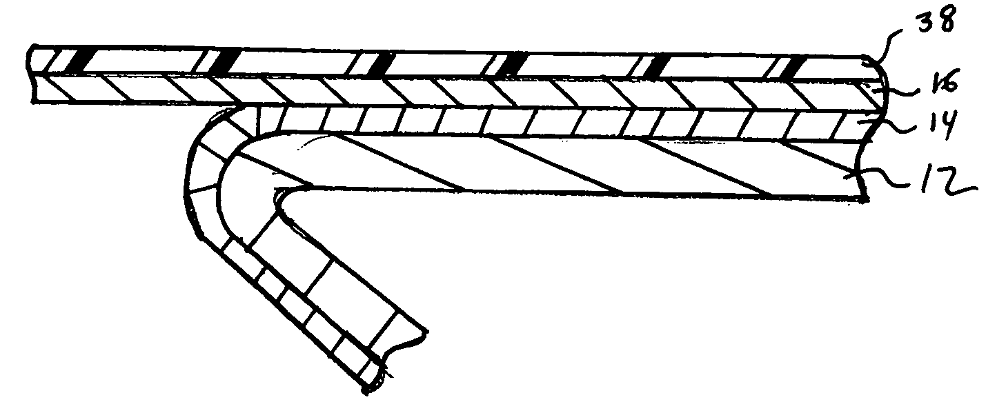
Support layer for thin copper foil
- Summary
- Abstract
- Description
- Claims
- Application Information
AI Technical Summary
Benefits of technology
Problems solved by technology
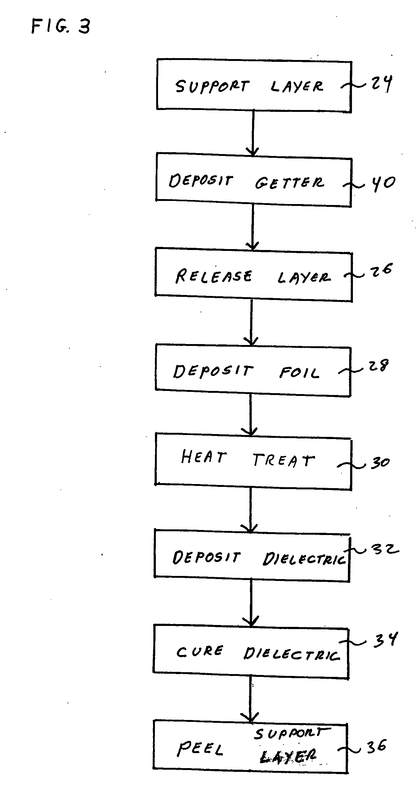
Method used
Image

Examples
example
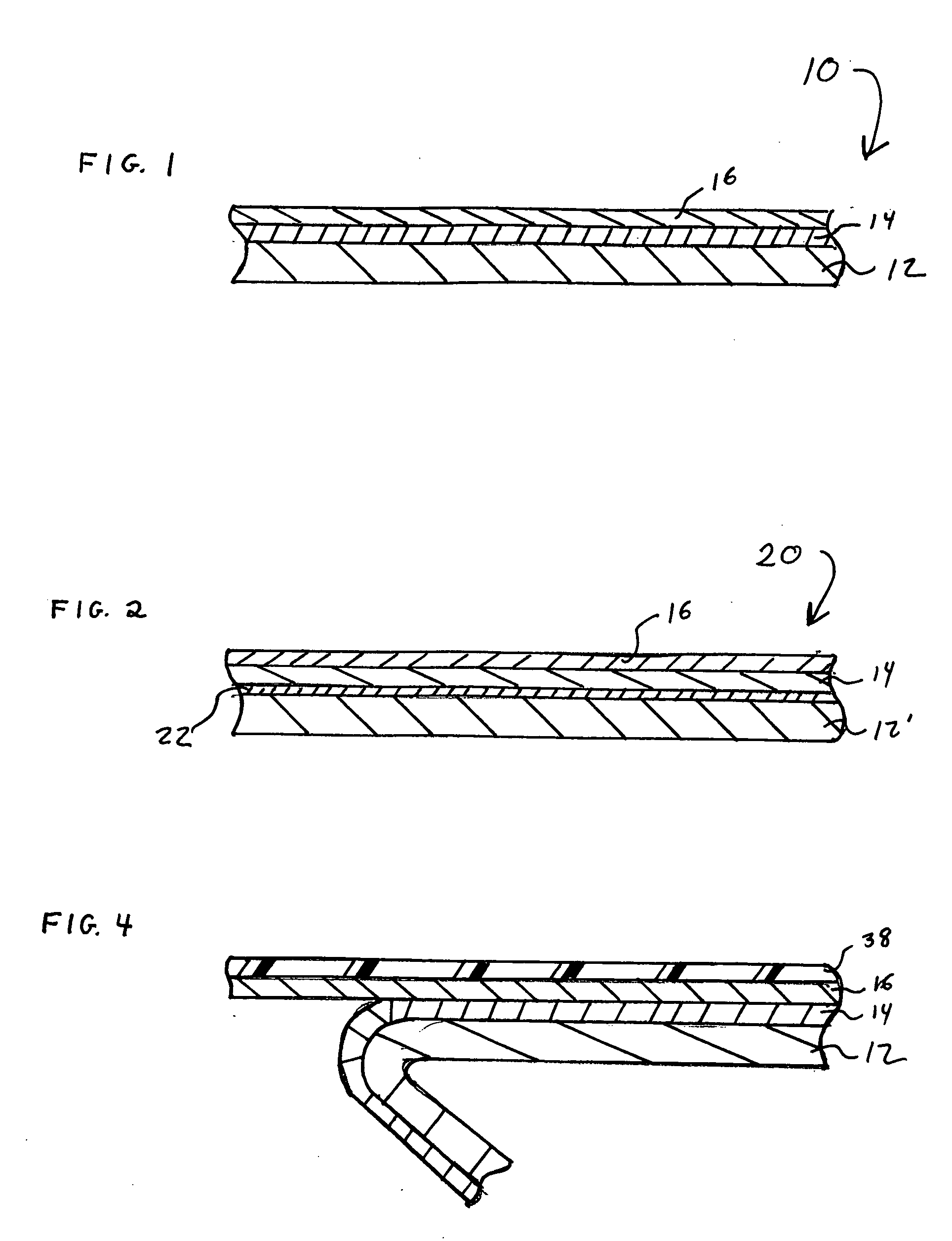
[0029] Support layers having the compositions and thicknesses recited in Table 1 were coated with a release layer having a thickness of between about 12 Å and about 200 Å and a nominal composition that was a mixture of chromium oxides, chromium, and chromium hydroxides. The release layer was deposited by electrodeposition. A copper foil layer having a nominal thickness of 5 μm was deposited by electrodeposition. The so-formed composite was then heated to 170° C. in an air, nitrogen or forming gas atmosphere for the time recited in Table 1.
[0030] The annealed samples were then heated to 360° C. for 30 minutes in a nitrogen atmosphere to simulate a cure cycle for a dielectric. The occurrence and density of blisters was then rated qualitatively to anticipate the quality of imaged copper foil circuit traces on a circuit board, where: 00=excellent; 0=good; Δ=fair; X=poor; and N.R.=not rated. The results are reported in Table 1.
TABLE 1Rating following a heat treatment for theSupportspe...
PUM
| Property | Measurement | Unit |
|---|---|---|
| Temperature | aaaaa | aaaaa |
| Temperature | aaaaa | aaaaa |
| Temperature | aaaaa | aaaaa |
Abstract
Description
Claims
Application Information
 - R&D Engineer
- R&D Manager
- IP Professional
- Industry Leading Data Capabilities
- Powerful AI technology
- Patent DNA Extraction
Browse by: Latest US Patents, China's latest patents, Technical Efficacy Thesaurus, Application Domain, Technology Topic.
© 2024 PatSnap. All rights reserved.Legal|Privacy policy|Modern Slavery Act Transparency Statement|Sitemap