Method of growing GaN crystal, method of producing single crystal GaN substrate, and single crystal GaN substrate
a technology of gan crystal and gan film, which is applied in the direction of crystal growth process, polycrystalline material growth, chemically reactive gases, etc., can solve the problems of difficult separation of sapphire substrates from gan films, inability to make gan single crystals, and inability to eliminate sapphire substrates which are chemically stable and physically rigid
- Summary
- Abstract
- Description
- Claims
- Application Information
AI Technical Summary
Benefits of technology
Problems solved by technology
Method used
Image
Examples
embodiment 1
[Embodiment 1]
1. Growth of GaN Layers on Undersubstrates
[1. Preparation of Undersubstrates]
[0137] A plurality of three kinds of undersubstrate S1, S2, S3 are prepared. All the three kinds of undersubstrate have circular wafers of a 51 mm (2 inches) diameter. [0138] S1. (0001) sapphire (Al2O3) wafer (top surface is a C-plane) [0139] S2. (111) GaAs wafer (top surface is a Ga-surface; A-plane) [0140] S3. (0001) GaN / sapphire wafer (1.5 μm GaN+sapphire) which has been made by coating a 51 mmφ sapphire wafer on which a 1.51 μm-thick GaN film has been grown by an MOCVD method.
[2. Formation of Dotted Seeding Mask]
[0141] Silicon oxide (SiO2) films of a 0.1 μm thickness are deposited by a plasma CVD method on the three kinds of the undersubstrates. The mask consists of dotted round seeds regularly populated on the undersubstrate.
[0142] The mask seeds are made by photolithography, which has steps of coating the SiO2 / undersubstrates with a resist, exposing the resist via four different st...
example 1 (
TEM OBSERVATION)
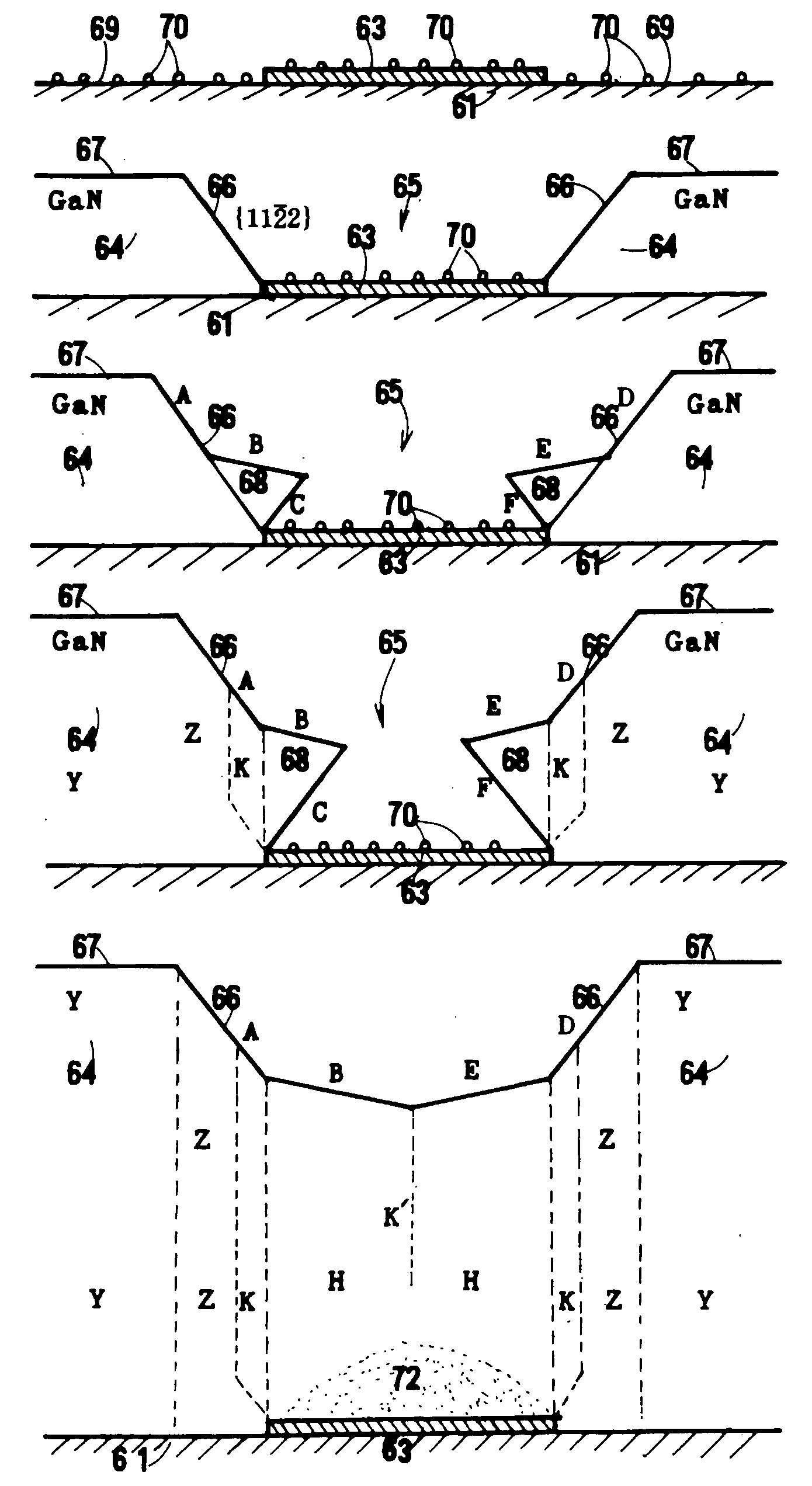
[0226] A GaN wafer made by the method of the present invention shows dislocation distribution on H, Z and Y as follows. [0227] H; 1×107 cm−2-2×107 cm−2 [0228] Z; 1×105 cm−2-1×107 cm−2 [0229] Y; 2×104 cm−2-2×105 cm−2
example 2 (
TEM OBSERVATION)
[0230] Another GaN wafer made by the method of the present invention shows dislocation distribution on H, Z and Y as follows. [0231] H; 5×107 cm−2-1×108 cm−2 [0232] Z; 3×105 cm−2-3×107 cm−2 [0233] Y; 2×105 cm−2-1×106 cm−2
[0234] Dislocation density fluctuates even in the same regions of H, Z and Y in a sample. In general, H has the highest density.
[0235] The closed defect accumulating region (H) is anomalous regarding dislocation density. H has dislocations more than Y and Z (H>Y, H>Z). In the H region, the dislocation density is 5×106 cm−2 to 5×108 cm−2. More than 50% of the Z region has low dislocations less than 5×106 cm−2. More than 60% of the Y region has low dislocations less than 5×106 cm−2. General tendency is H>Z>Y in dislocations.
TABLE 8Dislocation densityClosedAccompanyingdefectlow dislocationExtra lowZ / Haccumulatingsingle crystaldislocation singleorRegionregion (H)region (Z)crystal region (Y)Y / HDislocation5 × 106-6 (cm−2)6 (cm−2)10−3-density5 × 108(mor...
PUM
| Property | Measurement | Unit |
|---|---|---|
| temperature | aaaaa | aaaaa |
| temperature | aaaaa | aaaaa |
| temperature | aaaaa | aaaaa |
Abstract
Description
Claims
Application Information


