

Method for fabricating SiGe-on-insulator (SGOI) and Ge-on-insulator (GOI) substrates
a technology of ge-on-insulator and substrate, which is applied in the direction of solid-state devices, semiconductor devices, radio-controlled devices, etc., can solve the problems of poor bonding between the ge-containing layer and the buried insulator layer, and achieve the effect of reducing wavelength dependence, reducing effective absorption thickness of the ge-containing photodiode, and eliminating packaging problems
- Summary
- Abstract
- Description
- Claims
- Application Information
AI Technical Summary
Benefits of technology
Problems solved by technology
Method used
Image

Examples
Embodiment Construction
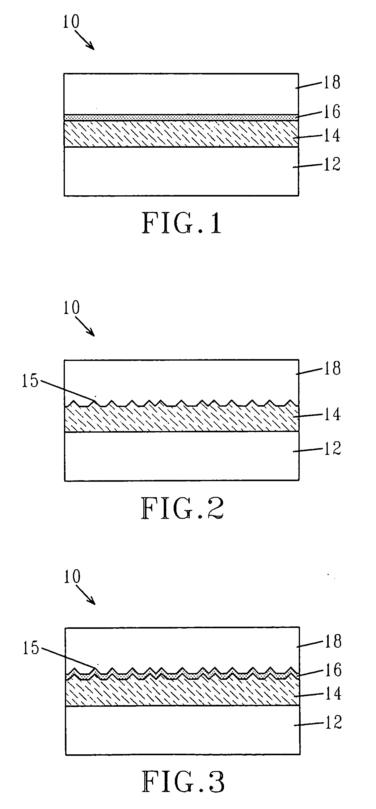
[0030] The present invention, which provides a method of fabricating a germanium-on-insulator (GOI) substrate material, the GOI substrate material itself, and structures including the GOI substrate material, will now be described in greater detail by referring to the following discussion together with the drawings that accompany the present application. In the accompanying drawings, like and / or corresponding elements are referred to by like reference numerals.
[0031] It is emphasized that the drawings of the present invention are not drawn to scale. For example, the roughened surfaces shown in the drawings are exaggerated for illustrative purpose. In reality, the roughened surfaces would be microscopic and would not be visible to the naked eye.
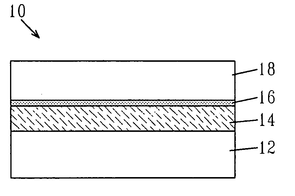
[0032] Reference is first made to FIG. 1, which illustrates one possible Ge-on-insulator (GOI) substrate material 10 of the present invention. Specifically, the GOI substrate material 10 comprises a substrate 12, a buried insulator layer 14 l...
PUM
 Abstract
Description
Claims
Application Information