Fabrication method of semiconductor integrated circuit device

a technology of integrated circuit devices and manufacturing methods, which is applied in the direction of individual semiconductor device testing, semiconductor/solid-state device testing/measurement, instruments, etc., can solve the problems of difficult to locate probes, not only breaking the natural oxide film formed over the surface of each test pad, but also forming a dent on the surface of the test pad, so as to reduce the damage of the test pad and shorten the electrical testing step

Inactive Publication Date: 2005-05-05
RENESAS TECH CORP
View PDF6 Cites 35 Cited by
  • Summary
  • Abstract
  • Description
  • Claims
  • Application Information

AI Technical Summary

Benefits of technology

[0008] In recent years, semiconductor integrated circuit devices have been discussed to perform many functions and a plurality of circuits tend to be integrated in one semiconductor chip (which will hereinafter simply be called a “chip”). In addition, a reduction in the manufacturing cost of semiconductor integrated circuit devices can be promoted by increasing the number of chips available from one wafer by miniaturizing the semiconductor elements and interconnects, while narrowing the area of the chip. In order to attain this, not only is the number of test pads (bonding pads) increased, but also these test pads are disposed at narrower pitches and the areas of the test pads are narrowed. With narrowing of the pitch of the test pads, it becomes difficult to locate probes so that they come into contact with the test pads when a prober having cantilever type probes is used for the probe testing.
[0010] In addition, wiping of the probe on the surface of the test pad shaves off a portion of the test pad, and shavings thus generated adhere to the tip portion of the probe. The shavings adhere to the tip portion of the probe one after another by the repetition of probing, which finally disturbs the electrical connection between the probe and the test pad. After probing is conducted a predetermined number of times, the probe should be cleaned by rubbing the tip portion of the probe with a certain cleaning sheet. The inevitable addition of this cleaning step prolongs the probe testing step, which also prolongs the fabrication time of the semiconductor integrated circuit device, resulting in a rise in the production cost of the semiconductor integrated circuit device.
[0013] At present, a method of reducing the number of test pads to be brought into contact with probes has been investigated utilizing DFT (Design For Testability) or BIST (Built In Self Test). Use of DFT (Design for Testability) or BIST (Built In Self Test) however needs disposal of new test pads. For the purpose of preventing elements or interconnects from being damaged by the impact upon contact of the probe with the test pad, the test pad is disposed in an input / output region having neither elements nor interconnects formed therebelow. With an increase in the operation speed of a semiconductor integrated circuit device, on the other hand, there is a growing need for disposal of a large number of power supply pads in their input / output regions in order to reduce noise (to reduce source impedance). In a chip of limited size, the size of each input / output region is also limited. The disposal of the power supply pads therefore makes it difficult to keep a region for the disposal of the above-described test pad that is used for DFT or BIST.
[0015] Another object of the invention is to provide, upon testing of a semiconductor integrated circuit device, a technique that is capable of reducing damage to the test pads.
[0016] A further object of the invention is to provide a technique that is capable of shortening the electrical testing step in the fabrication of a semiconductor integrated circuit device.
[0178] The present invention makes it possible to carry out electrical testing (probe testing) of a semiconductor integrated circuit device having test pads disposed at narrow pitches.

Problems solved by technology

With narrowing of the pitch of the test pads, it becomes difficult to locate probes so that they come into contact with the test pads when a prober having cantilever type probes is used for the probe testing.
Wiping of the probes will not only break the natural oxide film formed over the surface of each test pad, but also forms a dent on the surface of the test pad.
This leads to a problem in that the adhesive force of a bonding wire connected to the test pad in the later step is inevitably lowered.
There is also a fear that, as the area of the test pad decreases, the tip portion of the probe deviates from the test pad and a short-circuit occurs between the two test pads.
The shavings adhere to the tip portion of the probe one after another by the repetition of probing, which finally disturbs the electrical connection between the probe and the test pad.
The inevitable addition of this cleaning step prolongs the probe testing step, which also prolongs the fabrication time of the semiconductor integrated circuit device, resulting in a rise in the production cost of the semiconductor integrated circuit device.

Method used


Image

  • Fabrication method of semiconductor integrated circuit device
  • Fabrication method of semiconductor integrated circuit device
  • Fabrication method of semiconductor integrated circuit device

Examples


embodiment 1

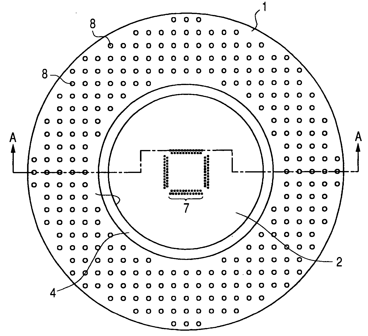
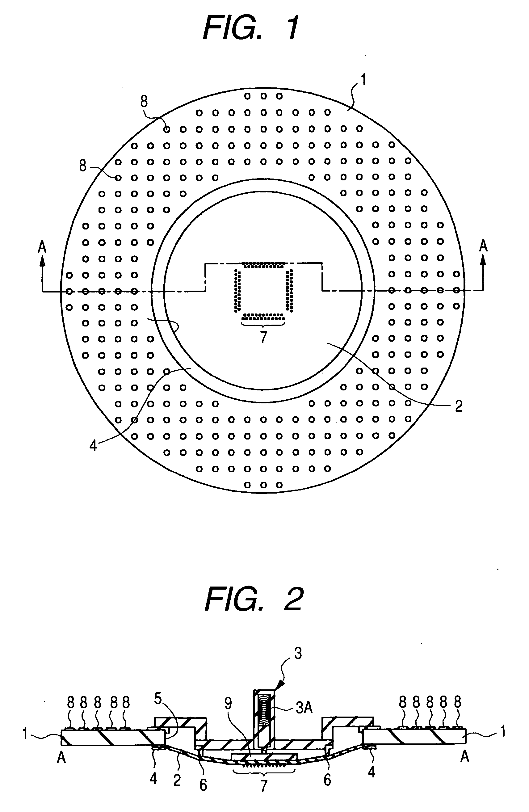
[0282]FIG. 1 is a fragmentary plan view of the lower surface of a probe card according to Embodiment 1, and FIG. 2 is a cross-sectional view taken along a line A-A of FIG. 1.

[0283] As illustrated in FIGS. 1 and 2, the probe card (first card) of Embodiment 1 is made of, for example, a multilayer wiring substrate 1, a thin film sheet (thin film probe (first sheet)) 2 and a plunger (pressing mechanism) 3. The thin film sheet 2 is fixed to the lower surface of the multilayer wiring substrate 1 by a presser ring 4, and the plunger 3 is attached to the upper surface of the multilayer wiring substrate 1. An opening portion 5 is located at the center of the multilayer wiring substrate 1, and, in this opening portion 5, the thin film sheet 2 and the plunger 3 are bonded via an adhesive ring 6.

[0284] Over the lower surface of the thin film sheet 2, a plurality of probes (contact terminals) 7, for example, having a pyramid form or trapezoidal pyramid form are provided. In the thin film sheet...

embodiment 2

[0315] A description will next be made of Embodiment 2.

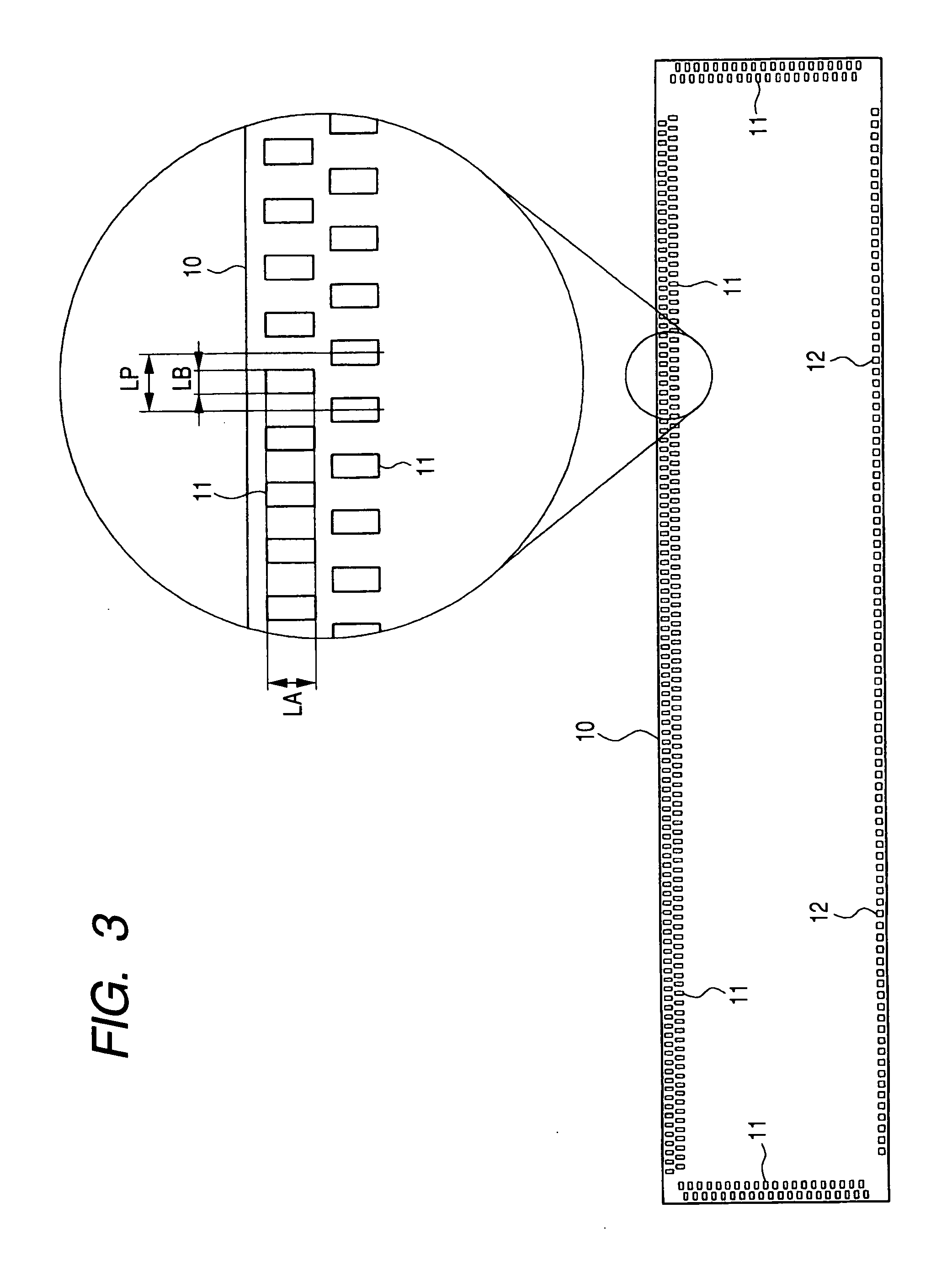
[0316] A relatively high current flows in some of the pads 11 and 12, which were described with reference to FIG. 3 in conjunction with Embodiment 1. When all of the probes 7A or 7B have the same size, an electrical load applied to the probe 7A or 7B to be brought into contact with the pad 11 or 12 through which a relatively high current flows increases. With an increase in the electrical load, the probe 7A or 7B which becomes hot may inevitably be welded with the pad 11 or 12 or the probe 7A or 7B may be broken. In Embodiment 2, as illustrated in FIG. 36, a plurality of probes (first contact terminals) 7B (or probes (first contact terminals) 7A) are disposed for the metal film 21B (or metal film 21A) which is opposite to the pad 11 or 12 through which a relatively high current flows, and the total contact area (first contact area) of the probes 7B (or probes 7A) and the pad 11 or 12 through which a relatively high current flow...

embodiment 3

[0319] A description will next be made of Embodiment 3.

[0320] When the probes 7A or 7B (refer to FIGS. 6 to 8) as described in conjunction with in Embodiments 1 and 2 are brought into contact with the pad 11 or 12 (refer to FIG. 3), a force is applied to a flat portion of the tip portion of the probe 7A or 7B. When a great force is applied to the probe 7A or 7B and the area of this flat portion is small, the metal film 21A or 21B including the probe 7A or 7B may be embedded inevitably into the polyimide films 22 and 25 (refer to FIGS. 6 to 8). Also, when the load applied to the probe 7A or 7B is excessively large, crushing or wearing of the probes 7A and 7B themselves may occur. In Embodiment 3, therefore, the area of the flat portion of the tip portion of the probe 7A or 7B is widened within an extent not causing such inconveniences. This makes it possible to prevent the breakage of the probes 7A and 7B.

[0321] In Embodiment 3, not only the area of the flat portion of the tip port...


PUM


Abstract

To permit electrical testing of a semiconductor integrated circuit device having test pads disposed at narrow pitches probes in a pyramid or trapezoidal pyramid form are formed from metal films formed by stacking a rhodium film and a nickel film successively. Via through-holes are formed in a polyimide film between interconnects and the metal films, and the interconnects are electrically connected to the metal films. A plane pattern of one of the metal films equipped with one probe and through-hole is obtained by turning a plane pattern of the other metal film equipped with the other probe and through-hole through a predetermined angle.

Description

CROSS-REFERENCE TO RELATED APPLICATION [0001] The present application claims priority from Japanese patent application No. 2003-372323, filed on Oct. 31, 2003, the content of which is hereby incorporated by reference into this application. BACKGROUND OF THE INVENTION [0002] The present invention relates in general to technology for the manufacture of a semiconductor integrated circuit device, and, more particularly, to a technique that is effective when applied to electrical testing of a semiconductor integrated circuit device having a plurality of electrode pads disposed at narrow pitches. [0003] For example, in the burn-in test of a semiconductor device having a protruding electrode, using a semiconductor device testing apparatus having a plurality of pyramid-shaped contact terminals protruding toward the semiconductor device, at least one contact terminal is brought into contact, at the ridge line or slope thereof, with one of the protruding electrodes, thereby bringing the semic...

Claims


Application Information

Patent Timeline
Patent Type & Authority Applications(United States)
IPC IPC(8): G01R1/067G01R1/06G01R1/073G01R3/00G01R31/28H01L21/66H01L21/822H01L27/04
CPCG01R1/06711H01L2224/0603G01R1/07307G01R3/00H01L22/14H01L2924/014H01L2924/3011G01R1/06744H01L2224/05554H01L2224/05553H01L2224/45144H01L2224/48453H01L2224/48463H01L2224/49171H01L2924/00H01L22/00
Inventor OKAMOTO, MASAYOSHIHASEGAWA, YOSHIAKIMOTOYAMA, YASUHIROMATSUMOTO, HIDEYUKIYORISAKI, SHINGOHASEBE, AKIOSHIBATA, RYUJINARIZUKA, YASUNORIYABUSHITA, AKIRAMAJIMA, TOSHIYUKI
Owner RENESAS TECH CORP
Why Eureka
Try Eureka