Method of fabricating devices and observing the same

a technology of device and pattern, applied in the direction of recording strategy, semiconductor/solid-state device testing/measurement, instruments, etc., can solve the problems of reducing the yield of patterns and devices to be fabricated, degrading the reproducibility of fabrication, and affecting the quality of the device, so as to save time and cost, observe easily, and prepare samples easily

Inactive Publication Date: 2005-05-19
HITACHI LTD
View PDF9 Cites 22 Cited by
  • Summary
  • Abstract
  • Description
  • Claims
  • Application Information

AI Technical Summary

Benefits of technology

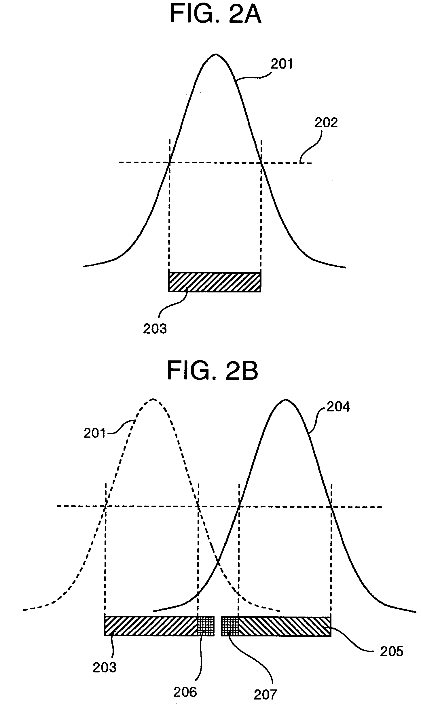
[0016] Conceivably, for avoidance of the inconvenience as above, the amount of irradiation of a beam is calculated in advance with a view to correcting power of the beam. In this method, however, power must sometimes be lowered drastically in order that a pattern of very high density can be produced. Accordingly, only partial power near the peak of gaussian beam distribution is used and in such an event, as the power of the beam varies, the pattern changes to a great extent. In other words, power margin of the beam is degraded. This leads to degraded reproducibility of fabrication to remarkably reduce the yield of patterns and devices to be fabricated.
[0037] According to the present invention, crystalline and amorphous patterns can be converted into an uneven pattern. In producing an amorphous pattern by melting crystal, a fine pattern can be prepared with high reproducibility by taking advantage of recrystallization occurring at a location distant from a central portion of a melting region. In addition, by using this technique, recorded marks in a phase-change optical disk can be observed cheaply within a short period of time.

Problems solved by technology

The conventional fabrication method for semiconductors and optical disk substrates is carried out with a system in which the reactivity of resist is proportional to the total irradiation amounts of a beam and in such a system, fineness of fabrication is limited.
This leads to degraded reproducibility of fabrication to remarkably reduce the yield of patterns and devices to be fabricated.

Method used


Image

  • Method of fabricating devices and observing the same
  • Method of fabricating devices and observing the same
  • Method of fabricating devices and observing the same

Examples


embodiment 1

[0087] A ROM substrate of an optical disk was fabricated using the method set forth so far.

[0088] A medium having a structure shown in FIG. 5A was fabricated and on trail, an amorphous mark was recorded by irradiating a laser beam on the medium. All of films stacked on a glass substrate 501 were formed through sputtering process. Protective films were of SiO2 and with a view to improving adhesiveness between lower SiO2 protective film 503 and recording film 505, a ZnS.SiO2 film 504 was interposed. A Ag layer 502 is adapted to diffuse heat generated in the recording film under the irradiation of the laser beam. This medium was heated at 300° C. for 3 minutes in a baking oven to crystallize the recording film 505 as shown at 507 in FIG. 5B. Under this condition, a laser beam having a wavelength of 400 nm was irradiated on the medium from upper part in the drawing through an objective lens of an numerical aperture of 0.9 so as to be focused on the recording film of the medium, so that...

embodiment 2

[0093] The present technique was used to produce on trial a thin line pattern with a laser beam.

[0094] A sample was prepared, having a structure as shown in FIG. 7A. This sample was placed in an oven and annealed at a temperature of 300° C. for 2 minutes to crystallize a recording film as shown at 704 in FIG. 7B. An ArF laser beam having a wavelength of 193 nm was focused on the sample through an objective lens having a numerical aperture of 0.8, so that while dissolving the recording film 704, a spot was scanned to produce an amorphous line and space (L&S) pattern 705 having a width of 50 nm. Laser power was 0.5 mW and the scanning speed was 1 m / s. The sample formed with the pattern is shown in sectional form in FIG. 7C and in top view form in FIG. 7D. Subsequently, an amorphous pattern 706 was recorded in the same manner as the pattern 705 in a direction orthogonal to the parallel pattern 705. At that time, the periphery of the pattern 706 was recrystallized. Accordingly, the pat...

embodiment 3

[0099] In this embodiment, production of a pattern by an electron beam was tried.

[0100] A medium was prepared, having a structure as shown in FIG. 8A. Recording film 802 and Si film 803 were formed on a Si substrate 801 by sputtering. The protective film was made of Si because conductivity was necessary for an electron beam to reach the recording film. In this embodiment, Ge2Sb2Te5 was used for the recording film.

[0101] The recording film of this sample was irradiated with the laser beam so as to be crystallized by half as shown in FIG. 8B. As a result, the recording film of the sample was bisected to crystalline region 804 and amorphous region 805.

[0102] An electron beam to be focused on the recording film was irradiated from upper part in the drawing in order that a pattern could be produced by Joule's heat generated by a current passing through the recording film. In the crystalline region 804, the recording film was molten with the electron beam subjected to 25 kV acceleratin...


PUM

PropertyMeasurementUnit
widthaaaaaaaaaa
sizeaaaaaaaaaa
sizeaaaaaaaaaa

Abstract

In fabricating process using a light beam or electron beam, reactivity is determined by the total amounts of photons or electrons absorbed by resist and consequently, fine fabrication cannot be achieved. On the other hand, thermal recording has been proposed but in the thermal recording, miniaturization of the fabrication size depends on a spot size of light beam or electron beam used for recording and is limited. Under the circumstance, to ensure a fine uneven pattern to be produced with high reproducibility, only crystal of a recording film used in a phase-change optical disk is peeled off by using an alkaline solution or pure water to leave only an amorphous portion on the sample surface and as a result, crystalline and amorphous patterns are converted into an uneven pattern.

Description

INCORPORATION BY REFERENCE [0001] The present application claims priority from Japanese application JP2003-332657 filed on Sep. 25, 2003, the content of which is hereby incorporated by reference into this application. BACKGROUND OF THE INVENTION [0002] The present invention relates to a method for micro-pattern fabrication and a method of observing an arrangement of atoms and molecules in a sample. [0003] In the process to fabricate a semiconductor, resist, having its reactivity changeable under irradiation of a laser beam or electron beam (EB), is coated on a substrate and after being irradiated with the laser beam or EB, the coated resist is developed so that an irradiated portion or unirradiated portion may be removed to produce an uneven pattern. In this case, a focusing optical system is used for the laser beam or EB and when taking the laser beam, for instance, a focused spot diameter can be written by λ / NA where λ represents the wavelength and NA represents the numerical aper...

Claims


Application Information

Patent Timeline
Patent Type & Authority Applications(United States)
IPC IPC(8): G03F7/00G11B7/0045G11B7/24G11B7/243G11B7/2433G11B7/26H01L21/00H01L21/66
CPCG11B7/00454G11B7/261G11B7/00456
Inventor SHINTANI, TOSHIMICHIANZAI, YUMIKOMINEMURA, HIROYUKIMIYAMOTO, HARUKAZU
Owner HITACHI LTD
Why Eureka
Try Eureka