Low temperature solder chip attach structure and process to produce a high temperature interconnection

a low temperature solder chip and interconnection technology, applied in the direction of soldering apparatus, sustainable manufacturing/processing, final product manufacturing, etc., can solve the problems of high cost of fabrication, inability to meet the requirements of high-temperature interconnection, so as to increase the reliability of the connection

Inactive Publication Date: 2005-05-26
INVENSAS CORP
View PDF35 Cites 6 Cited by
  • Summary
  • Abstract
  • Description
  • Claims
  • Application Information

AI Technical Summary

Benefits of technology

[0016] The present invention provides a process and structure for increasing the reliability of the connection between an area array package and a supporting substrate by providing a thin layer of Sn on the end of a Pb-rich ball, reflowing to form a eutectic interconnection, and annealing to diffuse the Sn into the Pb.

Problems solved by technology

The industry has moved away from the use of pins as connectors for electronic packaging due to the high cost of fabrication, the unacceptable percentage of failed connections which require rework, the limitations on input / output (I / O) density, and the electrical limitations of the relatively high resistance connectors.
Solder mounting is not a new technology.
One of the major drawbacks of this configuration is that the solder balls do not always remain in place before connection, during processing, or upon rework.
There is no guarantee, therefore, that the solder will remain associated with the first part during heating in subsequent processing.
Although it would seem that a low temperature flip chip would be desirable, this is not the case because the first level interconnection would reflow during subsequent second level attach (assuming a laminate chip carrier).
It is well known that the amount of molten solder in this type of flip chip interconnection can cause reliability problems, such as severe delamination.
Although the art of semiconductor chip to supporting substrate connections and packaging is well developed, there remain problems inherent in this technology, as described above.

Method used


Image

  • Low temperature solder chip attach structure and process to produce a high temperature interconnection
  • Low temperature solder chip attach structure and process to produce a high temperature interconnection
  • Low temperature solder chip attach structure and process to produce a high temperature interconnection

Examples


Embodiment Construction

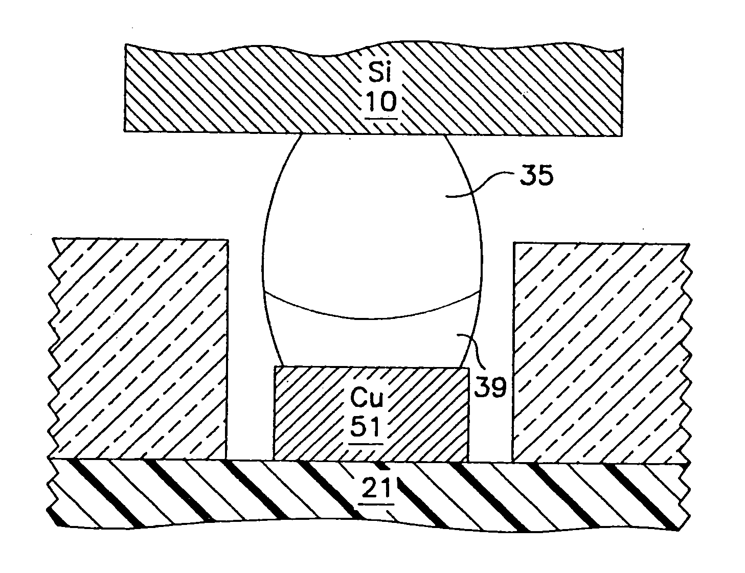
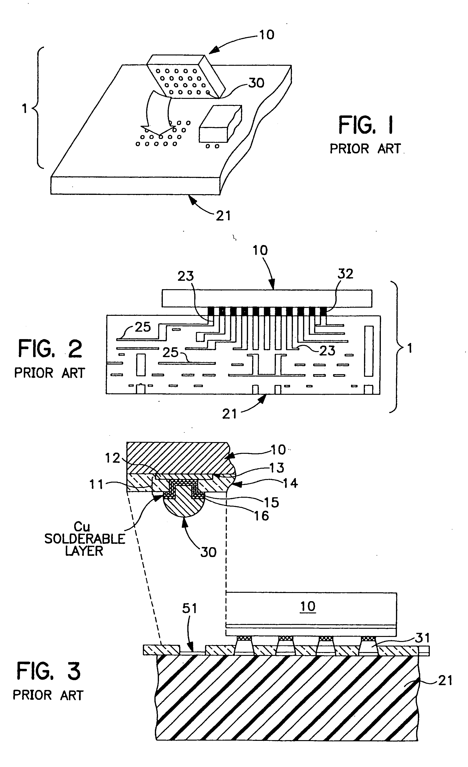
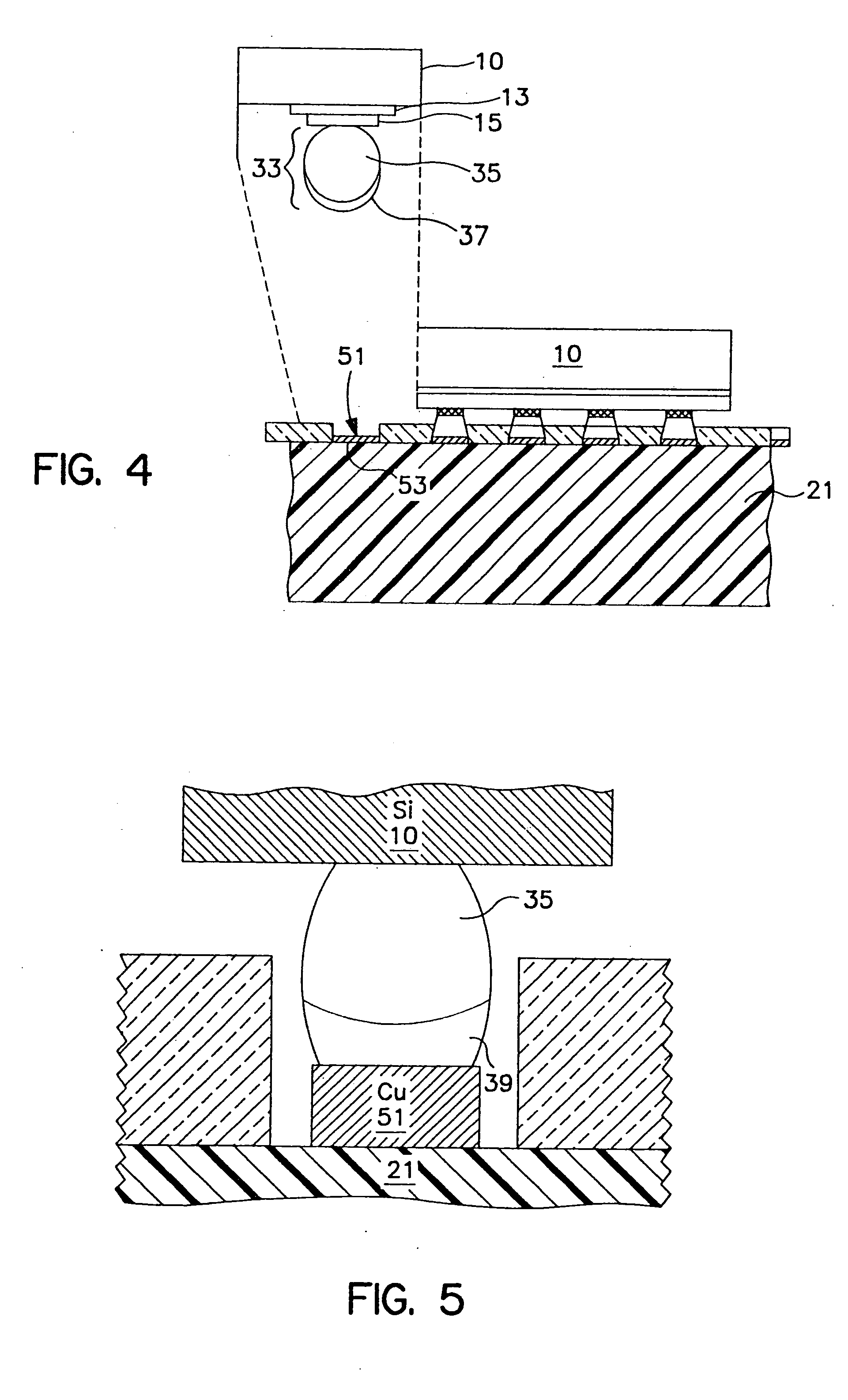
[0028] The present invention is directed to a process and structure for adhering a material to a supporting substrate. The present invention is used to join semiconductor chips, such as ball grid array (BGA) modules and flip chips, to a substrate, such as a printed circuit board (PCB), a microelectronic circuit card, or any organic or ceramic chip carrier or organic circuit board. A thin cap layer of a low melting point metal or alloy, preferably tin (Sn), is reflowed to form a eutectic alloy and annealed with a high melting point ball, preferably lead-rich. Sn and lead (Pb) will be used as the preferred materials in the following description of the embodiments, but any low melting point and high melting point eutectic system can be used. The annealing causes Sn from the eutectic alloy and any remaining unconsumed Sn from the thin cap layer of Sn to diffuse into the Pb in the ball, or vice versa, and thereby increase the melting temperature of the interconnection. This prevents refl...


PUM

PropertyMeasurementUnit
timeaaaaaaaaaa
timeaaaaaaaaaa
thicknessaaaaaaaaaa

Abstract

A solder interconnection uses preferably lead-rich solder balls for making a low temperature chip attachment directly to any of the higher levels of packaging substrate. After a solder ball has been formed using standard processes, a thin cap layer of preferably pure tin is deposited on a surface of the solder balls. An interconnecting eutectic alloy is formed upon reflow. Subsequent annealing causes tin to diffuse into the lead, or vice versa, and intermix, thereby raising the melting point temperature of the cap layer of the resulting assembly. This structure and process avoids secondary reflow problems during subsequent processing.

Description

FIELD OF THE INVENTION [0001] The present invention relates in general to a process and structure for adhering a material to a supporting substrate. In particular, the present invention describes a fabrication process and structure for attaching a chip or other substrate having a ball grid array to a chip carrier or printed circuit board. BACKGROUND OF THE INVENTION [0002] An electronic circuit contains many individual electronic circuit components, e.g., thousands or even millions of individual resistors, capacitors, inductors, diodes, and transistors. These individual circuit components are interconnected to form circuits, and the circuits are interconnected to form functional units. Microelectronic packages, such as chips, modules, circuit cards, circuit boards, and combinations thereof, are used to protect, house, cool, and interconnect circuit components and circuits. [0003] Within a single integrated circuit (IC), circuit component to circuit component and circuit to circuit i...

Claims


Application Information

Patent Timeline
Patent Type & Authority Applications(United States)
IPC IPC(8): B23K31/02B23K35/14B23K35/26H01L21/60H05K3/34
CPCB23K31/02H01L2924/014H01L24/11H01L24/81H01L2224/13099H01L2224/13111H01L2224/13609H01L2224/16H01L2224/81801H01L2924/01029H01L2924/01049H01L2924/01051H01L2924/01077H01L2924/01078H01L2924/01079H01L2924/01082H01L2924/01322H01L2924/14H01L2924/19041H01L2924/19042H01L2924/19043H05K3/3436H05K3/3463H05K2203/0435H05K2203/1105H01L2924/01005H01L2924/01006H01L2924/01024H01L2924/0105B23K35/268H01L2224/05001H01L2224/05027H01L2224/05022H01L2224/0508H01L2224/05572H01L24/05Y02P70/50
Inventor MILEWSKI, JOSEPH M.WOYCHIK, CHARLES G.
Owner INVENSAS CORP
Why Eureka
Try Eureka