Method and device for testing or calibrating a pressure sensor on a wafer

a technology of pressure sensor and wafer, which is applied in the direction of electronic circuit testing, measurement devices, instruments, etc., can solve the problems of complex and expensive testing of diced and housed pressure sensors, application of pressure sensors, etc., and achieve the effect of shortening the manufacturing process, avoiding the risk of future damage of these contacts, and reducing the size and production cost of the casing

Inactive Publication Date: 2005-06-02
FRAUNHOFER GESELLSCHAFT ZUR FOERDERUNG DER ANGEWANDTEN FORSCHUNG EV
View PDF17 Cites 23 Cited by
  • Summary
  • Abstract
  • Description
  • Claims
  • Application Information

AI Technical Summary

Benefits of technology

[0016] It is an advantage of the present invention that the pressure sensors can be tested or calibrated on the wafer not yet diced. This can take place simultaneously to a test of the electrical features of the integrated circuit or its functionality. Repeated handling, positioning and contacting the diced and housed pressure sensors are thus not required. Defect pressure sensors will not be housed since they have already been identified. Corresponding to the resulting simplification and shortening of the manufacturing process in the area of testing and calibrating, considerable cost advantages result which, as far as economics is concerned, enable the usage of integrated pressure sensors in many products. In addition, the present invention makes possible the usage of integrated pressure sensors in products in which testing or calibrating cannot be performed after dicing for technological reasons. The housed pressure sensor and its housing, respectively, need not comprise contacts for transferring calibration coefficients into an integrated memory element (such as, for example, an EEPROM). Thus, size and production cost of the casing can be produced and the risk of a future damage of these contacts can be avoided. A further advantage of the present invention is that it can be implemented by modifying a conventional wafer tester. The present invention thus only produces small investment cost.
[0017] A preferred field of application of the present invention is manufacturing absolute pressure sensors, in particular in a negative pressure range between 0 and 1 bar and, in particular, surface-micromechanical absolute pressure sensors in high numbers and, in particular, for fields of application in which the customer, after inserting the absolute pressure sensor into an entire system, does not have the possibility for calibrating the sensor.

Problems solved by technology

This procedure has the disadvantage that defect pressure sensors are housed, too, since their defect will only be recognized after dicing and housing.
In addition, testing the diced and housed pressure sensors is complicated and expensive since every single pressure sensor must be handled, positioned and contacted.
Thus, cost reasons prevent an application of pressure sensors in a number of products.
In some products, the calibration described cannot be performed after dicing and housing for technological reasons.
A further disadvantage is that, for storing or programming calibration coefficients or calibration parameters into the pressure sensor or the integrated circuit of it or an integrated memory element (such as, for example, an EEPROM), the case may have to have one or several additional contacts which are only used once, that is when calibrating the pressure sensor, which, however, increases the production cost and increases the danger of damage or destruction of it during the entire life time of the pressure sensor.

Method used


Image

  • Method and device for testing or calibrating a pressure sensor on a wafer
  • Method and device for testing or calibrating a pressure sensor on a wafer
  • Method and device for testing or calibrating a pressure sensor on a wafer

Examples


Embodiment Construction

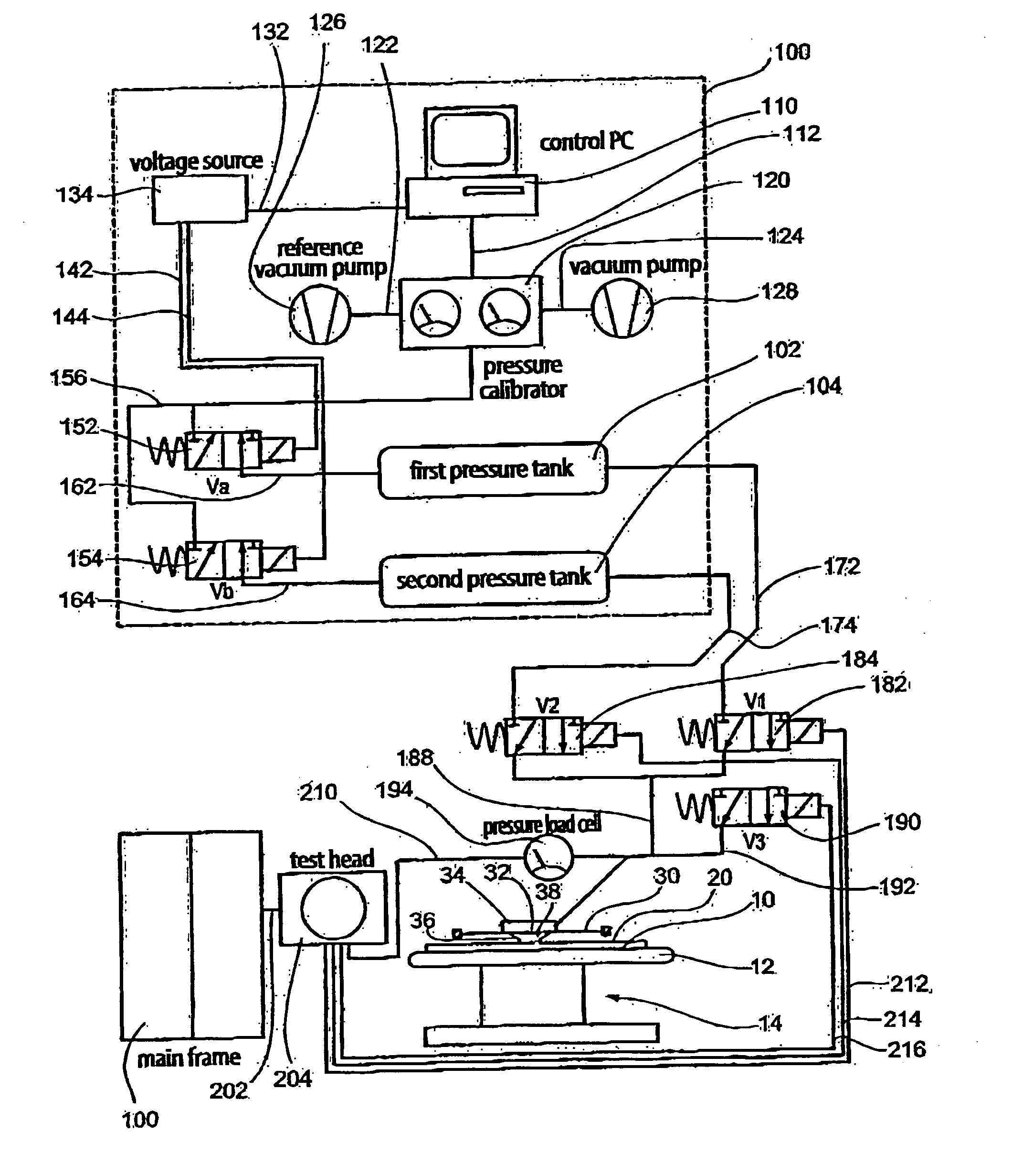
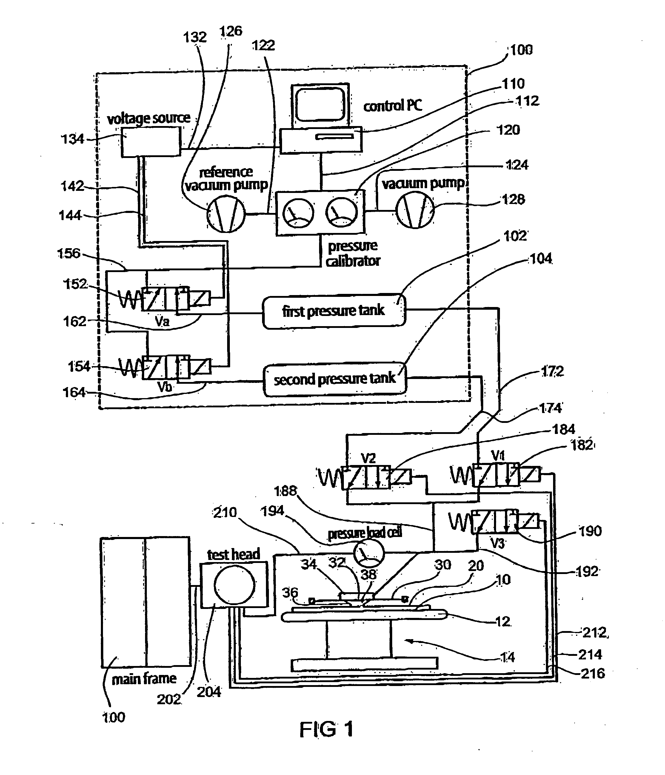
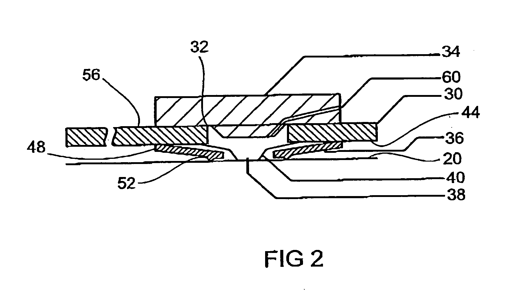
[0023] In FIG. 1, a schematic illustration of a testing system according to a preferred embodiment of the present invention is shown. A wafer 10 is held by a wafer carrier or chuck 12 of a prober 14 by means of a negative pressure, electrostatically or by means of an adhesive layer and is positioned in all three space directions. On a surface 20 of the wafer 10, a plurality of non-illustrated pressure sensors preferably having the same setup among one another and arranged in a regular raster are arranged. Each pressure sensor includes a pressure-sensitive portion, a mechanical-electrical transducer and a signal output.

[0024] In the case of a piezoelectric pressure sensor, the mechanical-electrical transducer is a solid body containing a piezo-effect, such as, for example, a piezoelectric crystal having a surface representing the pressure-sensitive portion of the pressure sensor.

[0025] In the case of a capacitive pressure sensor, the mechanical-electrical transducer is a capacitor,...


PUM

PropertyMeasurementUnit
pressureaaaaaaaaaa
pressureaaaaaaaaaa
angleaaaaaaaaaa

Abstract

A method is provided for testing or calibrating a pressure sensor of a plurality of pressure sensors formed in a wafer, wherein the pressure sensor has a pressure-sensitive portion and a signal output. The method includes a step of connecting the pressure-sensitive portion of the pressure sensor to a fluid line in a pressure-tight way, a step of applying a predetermined pressure to the pressure-sensitive portion of the pressure sensor via the fluid line and a step of receiving a signal from the signal output of the pressure sensor.

Description

CROSS-REFERENCE TO RELATED APPLICATION [0001] This application is a continuation of copending International Application No. PCT / EP02 / 06350, filed on Jun. 10, 2002, which designated the United States and was not published in English.BACKGROUND OF THE INVENTION [0002] 1. Field of the Invention [0003] The present invention relates to a method and a device for testing or calibrating a pressure sensor on a wafer. [0004] 2. Description of the Related Art [0005] Microelectronic circuits formed in or on a wafer are usually tested before dicing the wafer and housing the individual circuits. These tests are performed by automatic wafer probers or wafer testers. A wafer prober includes a handling system or handling means taking one individual wafer from a storage unit (rack) and passing it to the actual prober. The wafer is placed on a moveable carrier plate, the so-called chuck, and is fixed there by suction or electrostatically or with the help of an adhesive layer. The prober performs an ex...

Claims


Application Information

Patent Timeline
Patent Type & Authority Applications(United States)
IPC IPC(8): G01L27/00G01R31/02
CPCG01L27/005
Inventor KOESTER, OLIVERSLOTKOWSKI, JOHANN
Owner FRAUNHOFER GESELLSCHAFT ZUR FOERDERUNG DER ANGEWANDTEN FORSCHUNG EV
Why Eureka
Try Eureka