Method of fabricating substrate placing stage

a technology of substrate and placing surface, which is applied in the direction of metal-working equipment, metal-layered products, electrical equipment, etc., can solve the problems of reducing the temperature uniformity of semiconductors, difficult to fabricate one having uniform quality, and composite materials that are likely to produce warpage of substrate placing surfaces, etc., to reduce residual stress, reduce production of pores, and excellent joint strength

Active Publication Date: 2005-06-02
NGK INSULATORS LTD
View PDF6 Cites 40 Cited by
  • Summary
  • Abstract
  • Description
  • Claims
  • Application Information

AI Technical Summary

Benefits of technology

[0012] In accordance with the aspect, the ceramic base and the cooling member of the composite material are joined to each other with the joint layer including the aluminum alloy layer, mainly using a mechanical press-joining method without melting. The method eliminates production of pores caused by melting and solidification, obtaining excellent joint strength. The joining method ensures a thickness of the Al alloy layer, which is not achieved by brazing-solder joint. The Al alloy layer with a thickness in a range from 50 μm to 20

Problems solved by technology

The composite material, however, includes porous ceramics filled with metal, with difficulty to fabricate one having uniform quality because of the structural nature thereof.
For this reason, after being joined to the ceramic base by brazing solder, the composite material are likely to produce warpage of the substrate placing surface, variations in heat conductivity and the like due to the residual stress o

Method used


Image

  • Method of fabricating substrate placing stage
  • Method of fabricating substrate placing stage

Examples


examples

[0053] The following describes examples and comparative examples of the present invention.

examples 1 to 3

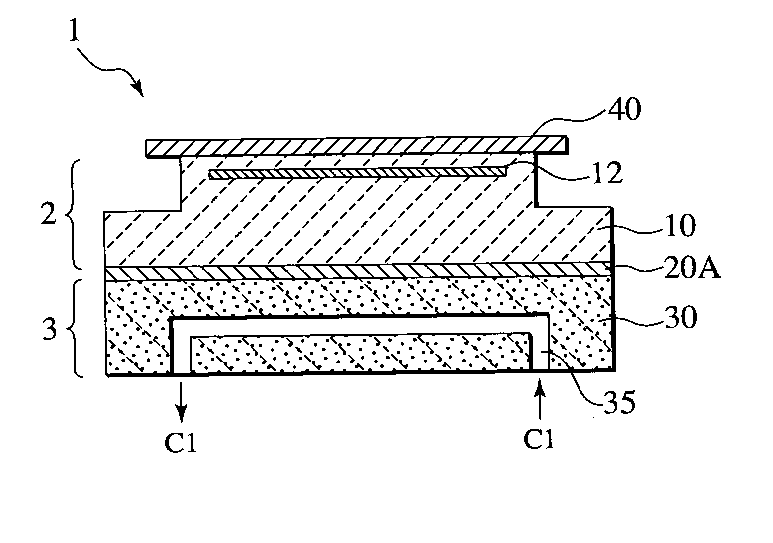
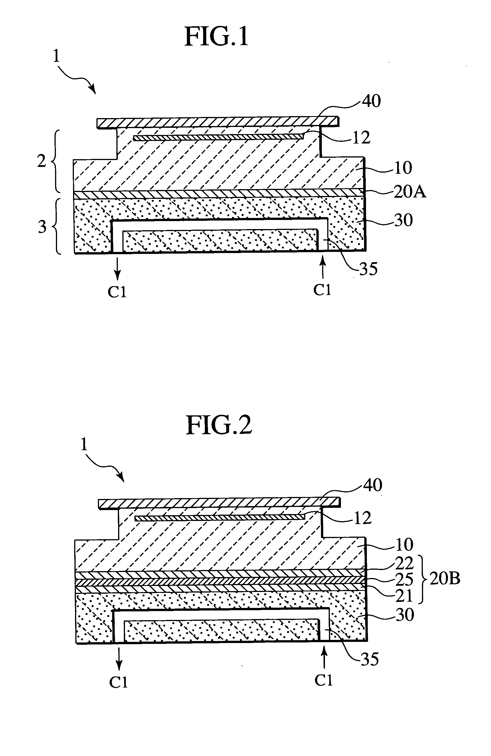
[0054] Firstly, a ceramic base having a function as an electrostatic chuck was fabricated. Specifically, an acrylic resin binder was added to aluminum nitride powder which was obtained by a reduction-nitridation method, and then granules were formed by a spray granulation method. In this granulation process, uniaxial pressure molding was performed by use of a die. In this molding process, a Mo bulk electrode which was a mesh electrode in the form of plate was embedded in a compact. This compact was subjected to hot press firing, thus fabricating an integrated sintered body. Pressure at the hot press process was set to 200 kg / cm2. During firing, the temperature was raised up to the maximum temperature of 1900° C. at a rate of 10° C. / hour, and then the maximum temperature was maintained for 1 hour. This fabricates a discoid aluminum nitride ceramic base having a diameter of 200 mm and a thickness of 10 mm. The ceramic base, after firing, is formed with through-holes each having an out...


PUM

PropertyMeasurementUnit
Thicknessaaaaaaaaaa
Thicknessaaaaaaaaaa
Thicknessaaaaaaaaaa

Abstract

A method of fabricating a substrate placing stage includes the step of providing a plate-shaped ceramic base having a substrate placing surface on a side of the ceramic base. The method includes the step of providing a plate-shaped ceramic base formed of a composite material containing components of a ceramic material and an aluminum alloy. The method includes the step of inserting a joint material including an aluminum alloy layer between the ceramic base and the cooling member. The method includes the step of heating the joint material at a temperature in a range from TS ° C. to (TS-30) ° C. (TS ° C.: a solidus temperature of the aluminum alloy). The method includes the step of pressing substantially normally joint surfaces of the ceramic base and the cooling member, thereby joining the ceramic base and the cooling member via the joint material to obtain a joint layer including the aluminum alloy layer having a thickness in a range from 50 μm to 200 μm after joining.

Description

CROSS-REFERENCE TO RELATED APPLICATIONS [0001] This application is based upon and claims the benefit of priority from Japanese Patent Application No. 2003-330493 filed on Sep. 22, 2003; the entire contents of which are incorporated herein by reference. BACKGROUND OF THE INVENTION [0002] The present invention relates to a substrate placing stage, more specifically, to a method of fabricating a substrate placing stage having a structure of joining a ceramic base and a cooling member together. [0003] Conventionally, the semiconductor fabricating process uses various substrate placing stages such as ceramic heaters or electrostatic chucks for placing semiconductor wafers. [0004] For example, a ceramic heater or an electrostatic chuck is structurized to embed an electrode in the form of a wire, a plate or a film inside a discoid ceramic base corresponding to the shape of a wafer. This is used to set the substrate to a predetermined temperature or to fix the wafer on the substrate placing...

Claims


Application Information

Patent Timeline
IPC IPC(8): H05B3/84B23K35/12B32B15/04C04B35/565C04B37/00H01L21/00H01L21/02H01L21/3065H01L21/68H01L21/683H05B3/10H05B3/18H05B3/74
CPCB23K35/0233Y10T428/12535B23K35/286B32B15/04C04B35/645C04B37/026C04B2235/656C04B2235/6581C04B2235/963C04B2237/121C04B2237/122C04B2237/343C04B2237/365C04B2237/366C04B2237/368C04B2237/402C04B2237/403C04B2237/708C22C29/065H01L21/67109B23K35/0238B32B15/043B32B2307/302B32B15/20
Inventor FUJII, TOMOYUKIIMAI, YASUYOSHIKAWAJIRI, TETSUYA
Owner NGK INSULATORS LTD
Why Eureka
Try Eureka