Ald deposition of ruthenium

a technology of ruthenium and ald, applied in the direction of chemical vapor deposition coating, semiconductor/solid-state device details, coatings, etc., can solve the problems of uniform deposition on some dielectric surfaces, inability to electroplate copper directly onto diffusion barrier materials without a thin copper seed layer, and no known solution for direct deposition of ruthenium

Inactive Publication Date: 2005-06-02
IBM CORP
View PDF13 Cites 71 Cited by
  • Summary
  • Abstract
  • Description
  • Claims
  • Application Information

AI Technical Summary

Benefits of technology

[0007] It is therefore an aspect of the present invention to provide a method for

Problems solved by technology

However, copper cannot be electroplated directly onto diffusion barrier materials without a thin copper seed layer.
However, due to a nucleation problem associated with the metal organic ruthenium precursor, only a very limited, non-uniform deposition occurs on some dielectric surfaces, including silicon dioxide (SiO2).
There has been no know solution for direct deposition of ruthenium by ALD on SiO2 and other dielectri

Method used


Image

  • Ald deposition of ruthenium
  • Ald deposition of ruthenium
  • Ald deposition of ruthenium

Examples


example

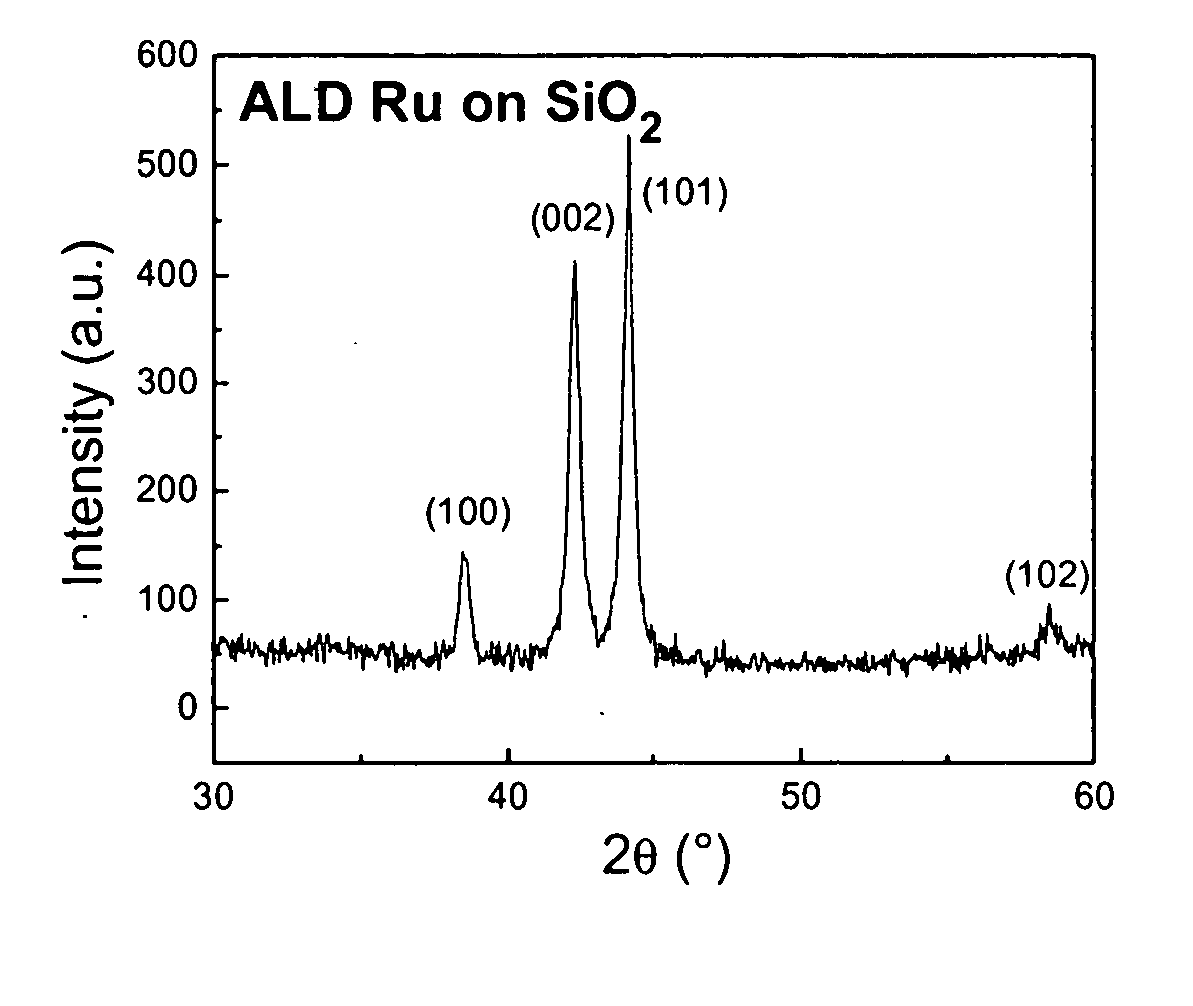
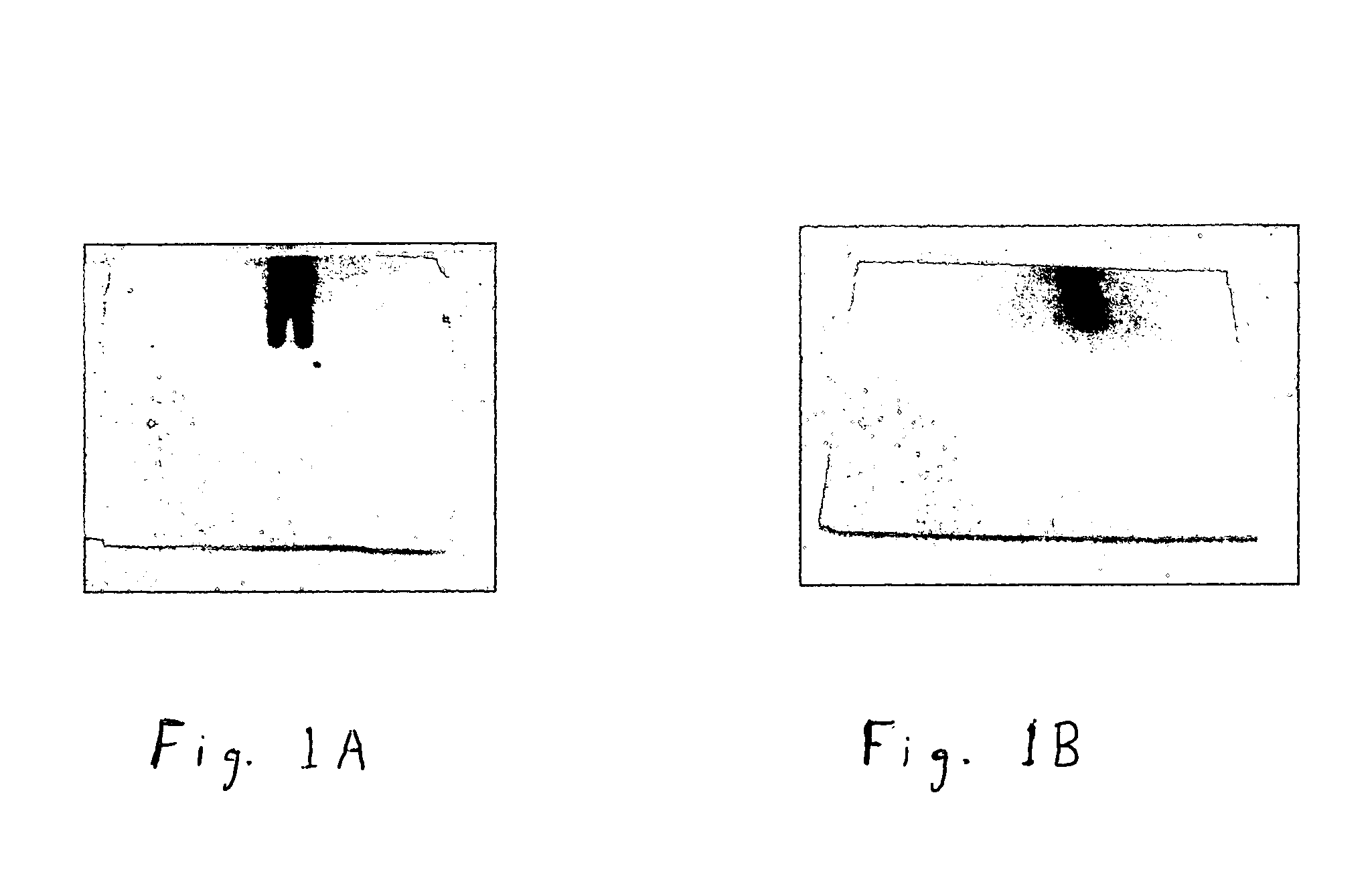
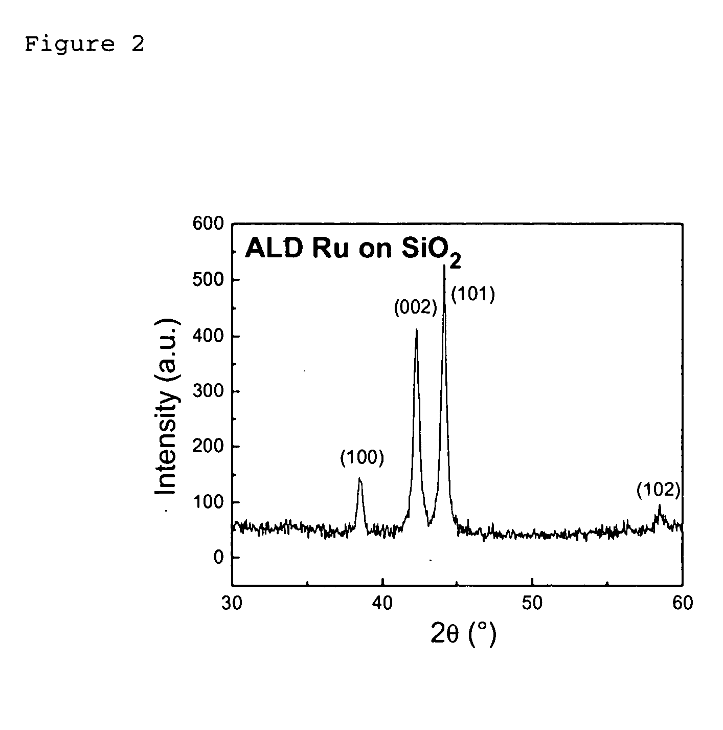
[0031] To deposit nucleation problem free ALD ruthenium on SiO2, the substrates are exposed to the plasma prior to the ALD of ruthenium for 10 minutes at the deposition temperature. Nitrogen, oxygen and hydrogen plasma may be used at 500 Watts of plasma power. In general, hydrogen plasma exposure does not, in and of itself, produce any significant improvement in terms of producing a uniform layer. However, oxygen plasma exposed SiO2 produces very uniform, clean looking deposition on the substrates. Eight inch (20.3 cm) SiO2 wafers are used for measurements of uniformity. In terms of sheet resistance, the uniformity of the deposited ruthenium films exhibits less than 5% variation in sheet resistance, without any bare surface spots. Similar improvement is also obtained by nitrogen exposure for 10 minutes on SiO2 substrates. The clean, macroscopic defect free ruthenium metal films deposited by ALD is shown in FIG. 1b.


PUM

PropertyMeasurementUnit
Temperatureaaaaaaaaaa

Abstract

A method to deposit nucleation problem free ruthenium by ALD. The nucleation problem free, relatively smooth ruthenium ALD film is deposited by the use of plasma-enhanced ALD of ruthenium underlay for consequent thermal ruthenium ALD layer. In addition, oxygen or nitrogen plasma treatments of SiO2 or other dielectrics leads to uniform ALD ruthenium deposition. The method has application as a direct plating layer for a copper interconnect or metal gate structure for advanced CMOS devices.

Description

FIELD OF THE INVENTION [0001] This invention relates to electrical interconnection structures. More particularly, it relates to “back end of the line” (BEOL) interconnections in high performance integrated circuits, and to advanced CMOS device fabrication. BACKGROUND OF THE INVENTION [0002] Electrodeposition of copper is a standard deposition technique used for copper interconnect applications. However, copper cannot be electroplated directly onto diffusion barrier materials without a thin copper seed layer. In current processes, the copper seed layers are deposited by Physical Vapor Deposition (PVD) for this purpose, often by derivative techniques of ionized PVD (I-PVD). However, in future semiconductor generations, a very conformal film deposition in nanoscale, high aspect ratio structures will be required. This may only be achievable only by Atomic Layer Deposition (ALD) techniques. As an alternative, copper electrodeposition can be also done on other low-resistance metal surface...

Claims


Application Information

Patent Timeline
IPC IPC(8): C23C16/18H01L21/285H01L21/768H01L23/532
CPCC23C16/18C23C16/45525C23C16/45529H01L23/53238H01L21/28562H01L21/76843H01L21/76873C23C16/45542H01L2924/0002H01L2924/00
Inventor KIM, HYUNGIUNROSSNAGEL, STEPHEN M.
Owner IBM CORP
Why Eureka
Try Eureka