Method for forming metal wires by microdispensing pattern

a technology of metal wires and patterns, applied in the field of forming metal wires, can solve the problems of reducing the reliability of the substrate, affecting the quality of the substrate, so as to enhance the homogeneous distribution of pd nucleation, improve the surface properties, and effectively absorb the effect of a catalytic agen

Inactive Publication Date: 2005-06-09
IND TECH RES INST
View PDF6 Cites 32 Cited by
  • Summary
  • Abstract
  • Description
  • Claims
  • Application Information

AI Technical Summary

Benefits of technology

[0010] The invention modifies the surface properties by forming a self-assembled monolayer (SAM) interface on the substrate surface. The SAM layers treat the surface has a special nanometer interface structure due to the chemical dynamics difference among the atoms. The layers structure has a nanometer thickness coating on the surface. The film forming mechanism of the SAM is the chemical adsorption at the interface between the solid and liquid phases. A two-dimensional ordered molecular layer with atoms closely packed by chemical bonds. Controlling to form such SAM repeatedly can form a multi-layer interface structure at the nanometer scale. One can use the components, structure, physical and chemical properties of the film interface to change the surface properties of the substrate. The substrate surface is thus endowed with selective absorption abilities. Therefore, the substrate can effectively absorb a catalytic agent.
[0011] By microdispensing a catalytic agent at places to form metal wires, It needs several minutes to dry and Pd nucleation residual on surface. In this invention, to enhance this homogeneous distribution of Pd nucleation, a vibration device likes PZT is operated beneath on the substrate during drying period. Besides, by electroless plating, the width and thickness of the metal wire can be controlled and its resistance can be reduced. The combination of microdispensing and electroless plating can shorten the metal wire preparation time and increase its yield in comparison with the conventional photolithography and etching processes.

Problems solved by technology

These methods suffer from the drawback of being analogue processes and hence require conversion from a digital data file to converted printable image via initial production of a screen or photo tool.
This adds cost and time delays to the preparation of boards particularly prototype and short run board production.
This is incompatible with the rule that halide are forbidden in all electronic products set by the Europe standard in 2004.
This makes the substrate have worse dielectric and insulating properties and be likely to deform at high temperatures.
All such facts will reduce the reliability of the substrate.
This inevitably increases the manufacturing costs.

Method used


Image

  • Method for forming metal wires by microdispensing pattern
  • Method for forming metal wires by microdispensing pattern
  • Method for forming metal wires by microdispensing pattern

Examples


Embodiment Construction

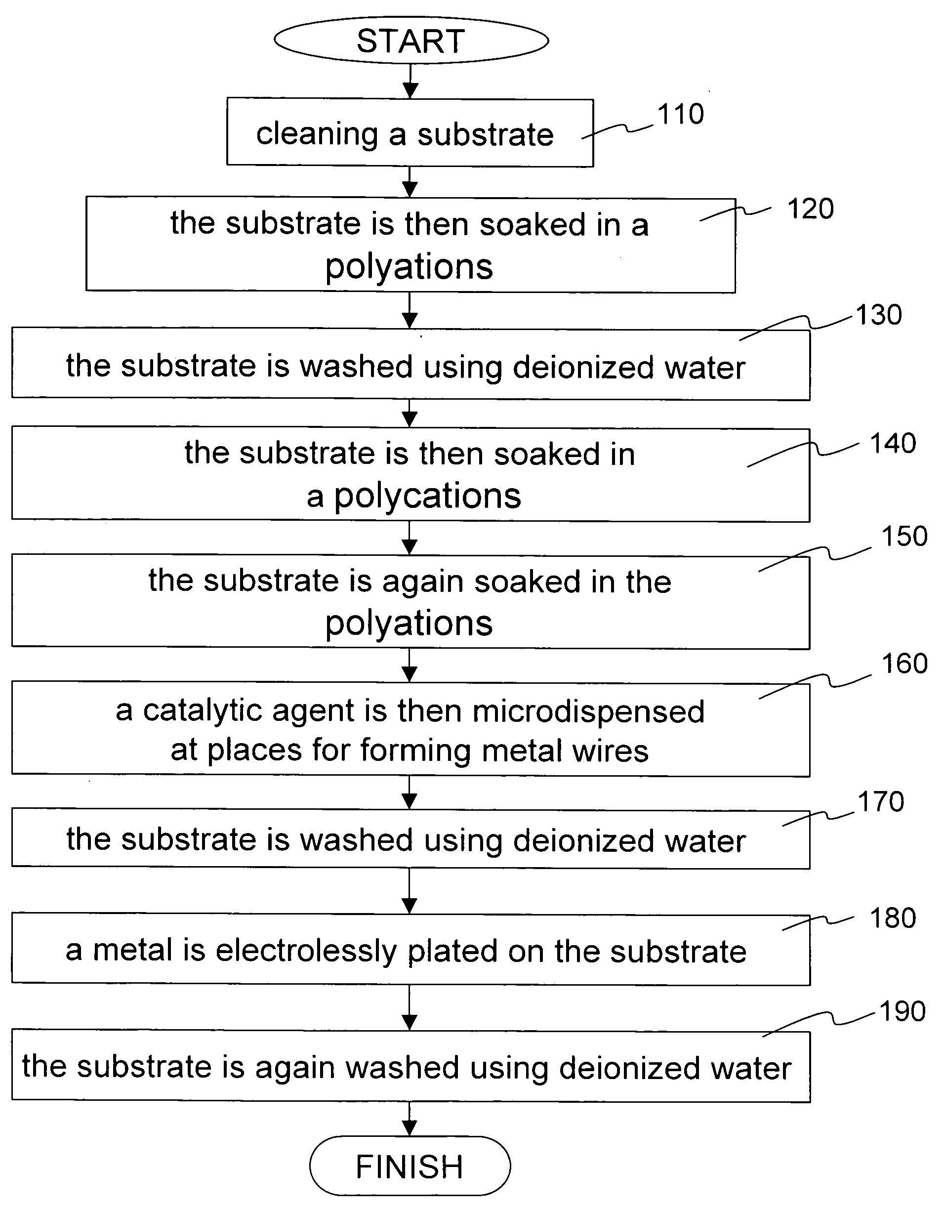
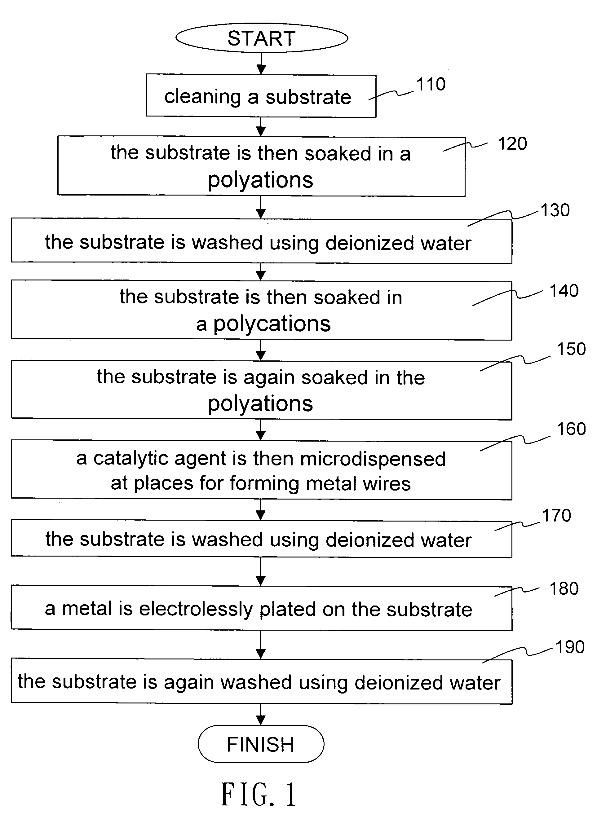
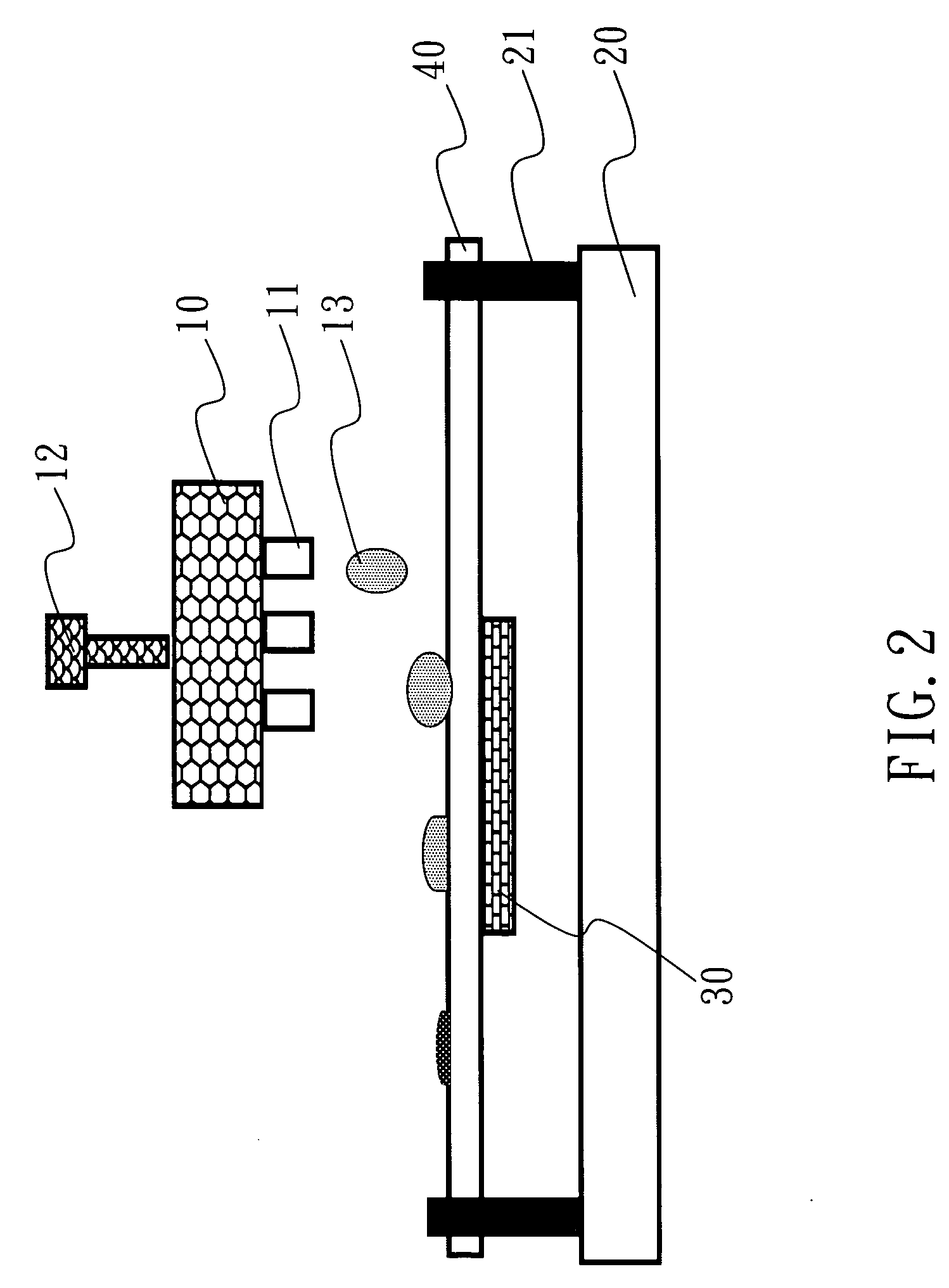
[0017] With reference to FIG. 1, the disclosed metal wire formation method starts by cleaning a substrate (step 110). It is done by a 10-minute UV-ozone treatment. The substrate is then soaked in a polyanions (step 120). The polyanions is a 10 milli-M polyacrylic acid (PAA). Afterwards, the substrate is washed using deionized water (step 130). The substrate is then soaked in a polycations (step 140). The polycations is a 10 milli-M polyallylamine hydrochloride (PAH). The substrate is again soaked in the polyanions solution (step 150). A catalytic agent is then microdispensed at places for forming metal wires (step 160). The catalytic agent is a 10 milli-M sodium tetrachloropalladate (Na2PdCl4) solution. Afterwards, the substrate is washed using deionized water (step 170). The substrate is then soaked in a HCl solution with a pH value between 2.5 and 3 for 30 seconds. A metal is electrolessly plated on the substrate (step 180). Finally, the substrate is again washed using deionized w...


PUM

PropertyMeasurementUnit
flexibleaaaaaaaaaa
temperatureaaaaaaaaaa
frequencyaaaaaaaaaa

Abstract

A method for forming metal wires by microdispensing a pattern is disclosed. The method includes the steps of microdispensing a catalyst pattern on the substrate and forming metal wires by electroless plating. Before the step of microdispensing catalyst pattern, the surface properties of the substrate have been improved by a surface modification treatment.

Description

BACKGROUND OF THE INVENTION [0001] 1. Field of Invention [0002] The invention relates to a method for forming metal wires and, in particular, to a method for forming metal wires by microdispensing a pattern on substrate. [0003] 2. Related Art [0004] Classical PCB processes include the step of dry metal film attach to substrate, spin photo resist, mask pattern & development, etching photo resist, the second metal plating, and cleaning resist etc. complex processes. For many years, screen-printing and photolithography have been the predominant methods of imaging in PCB manufacturing processes. These techniques have served the industry well and provided the desired image resolution at an acceptable cost. Both methods have their own individual strengths and weaknesses and manufacturers select the most appropriate process for their requirements in primary track imaging, solder mask application and legend printing. These methods suffer from the drawback of being analogue processes and hen...

Claims


Application Information

Patent Timeline
Patent Type & Authority Applications(United States)
IPC IPC(8): C23C18/16C23C18/18C23C18/30H01L29/10H05K3/18
CPCB82Y30/00Y10T29/49117C23C18/30H05K3/182H05K2203/013H05K2203/0709C23C18/1608C23C18/1806C23C18/1855C23C18/1893C23C18/2086Y10T29/49128Y10T29/49155Y10T29/49126C23C18/2006C23C18/204
Inventor CHENG, KEVINYANG, MING-HUANCHIU, WAN-WENCHANG, JANE
Owner IND TECH RES INST
Why Eureka
Try Eureka