
Plating method, plating apparatus and a method of forming fine circuit wiring

a plating apparatus and wire technology, applied in the field of copper plating methods, can solve the problems of reducing the electric conductivity of copper plating films, affecting the production efficiency of printed circuits, so as to reduce the amount of chlorine ions incorporated, improve the electromigration resistance, and reduce the possibility of corrosion and deterioration of copper-plated wiring.

Inactive Publication Date: 2005-06-16
EBARA CORP +1
View PDF10 Cites 20 Cited by
  • Summary
  • Abstract
  • Description
  • Claims
  • Application Information

AI Technical Summary

Benefits of technology

[0024] The use of any copper plating method, leveler or plating apparatus according to this invention makes it possible to reduce the amount of the chlorine ions incorporated in any copper plating film and thereby the possibility of corrosion and deterioration of any copper-plated wiring.
[0025] The fine circuit wiring formed by phosphorus-doped copper in accordance with this invention has a higher level of electromigration resistance than that of any wiring formed by copper alone, allows an electric current to pass therethrough at a higher current density and therefore copes with a demand for finer and higher density circuit wiring.

Problems solved by technology

While the chlorine ions play an important role in a plating solution as stated above, it has been a problem that the chlorine ions incorporated in a copper plating film lower its electric conductivity.
Another problem has been due to the corrosiveness of chlorine ions, as they cause the corrosion and deterioration of plated wiring.
Accordingly, copper wiring has come to be required to allow a steady flow of an electric current at a higher current density, but has come to present a problem of electromigration.
Electromigration is likely to cause the formation of voids in copper wiring or its insulation and thereby exert a serious effect on electronic devices.
Moreover, electromigration causes stress migration as a secondary phenomenon and is likely to increase the frequency of occurrence of the serious effect as stated above.
As tin is a metal which is electrochemically baser than copper, it has been difficult to form a deposited copper film containing tin uniformly by electroplating, since copper is deposited more actively than tin.
Accordingly, there has been no effective way to form copper wiring having a high level of electromigration resistance by copper plating.

Method used


Image

  • Plating method, plating apparatus and a method of forming fine circuit wiring
  • Plating method, plating apparatus and a method of forming fine circuit wiring
  • Plating method, plating apparatus and a method of forming fine circuit wiring

Examples


example 1

[0079] A test was conducted to ascertain that chlorine ions incorporated into a plating film were of a leveler.

[0080] One liter of a plating solution was so prepared as to contain 200 g of CuSO4.5H2O, 10 g of H2SO4, 60 mg of chlorine ions, 200 mg of polyethylene glycol having a molecular weight of about 3000 and 5 mg of bis(3-sulfopropyl)disulfide.

[0081] A quaternary ammonium hydrochloride salt of polyvinyl pyridine yet to be dechlorinated was employed as a leveler and was so added to the plating solution that the plating solution might contain 10 mg of polyvinyl pyridine per liter. The leveler yet to be dechlorinated contained 16 g of polyvinyl pyridine and 4 g of chlorine ions per liter. The plating solution was used for the copper plating of a silicon wafer. The plating solution to which no leveler had been added was also used for the copper plating of a silicon wafer.

[0082] The copper-plated silicon wafers were examined by a secondary ion mass spectrometer (SIMS) for the chlo...

example 2

[0084] The leveler used in Example 1 was dechlorinated to prepare a leveler having a chlorine ion concentration reduced to 1 g / l.

[0085] The dechlorinated leveler and the same plating solution as in Example 1 were used for the copper plating of a silicon wafer.

[0086] The examination of the wafer by SIMS as in Example 1 can confirm a reduction in the amount of chlorine ions incorporated in its copper plating film.

example 3

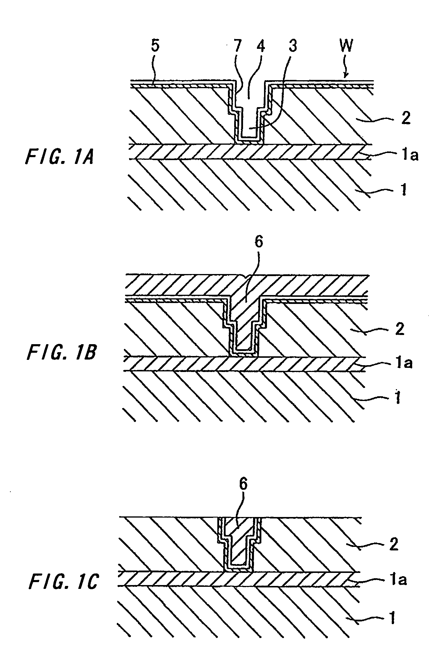
[0087] A phosphorus-doped copper plating solution was prepared by adding 5 ml of 50% phosphoric acid to one liter of a copper sulfate plating solution (basic solution) having the composition shown below. The plating solution was used for one minute of phosphorus-doped copper plating at a temperature of 25° C. and a current density of 30 mA / cm2 on a semiconductor wafer in which via holes having a width of 150 nm and an aspect ratio of 5 had been formed. The semiconduct or wafer had a barrier and a seed layer formed by customary methods.

[0088] Composition of the Copper Sulfate Plating Solution:

Copper sulfate pentahydrate200 g / lSulfuric acid 50 g / lChlorine ion 50 mg / lPhosphorus compound100 mg / l(as phosphoric acid ion)Polymer component 30 ml / lCarrier component 10 ml / lLeveler component 10 ml / l

[0089] There was obtained a phosphorus -doped copper plating film having a phosphorus content of 1×10⁻⁶ atom % or more along its depth. Its examination by a scanning electron microscope did not r...


PUM

PropertyMeasurementUnit
volume resistivityaaaaaaaaaa
current densityaaaaaaaaaa
temperatureaaaaaaaaaa

Abstract

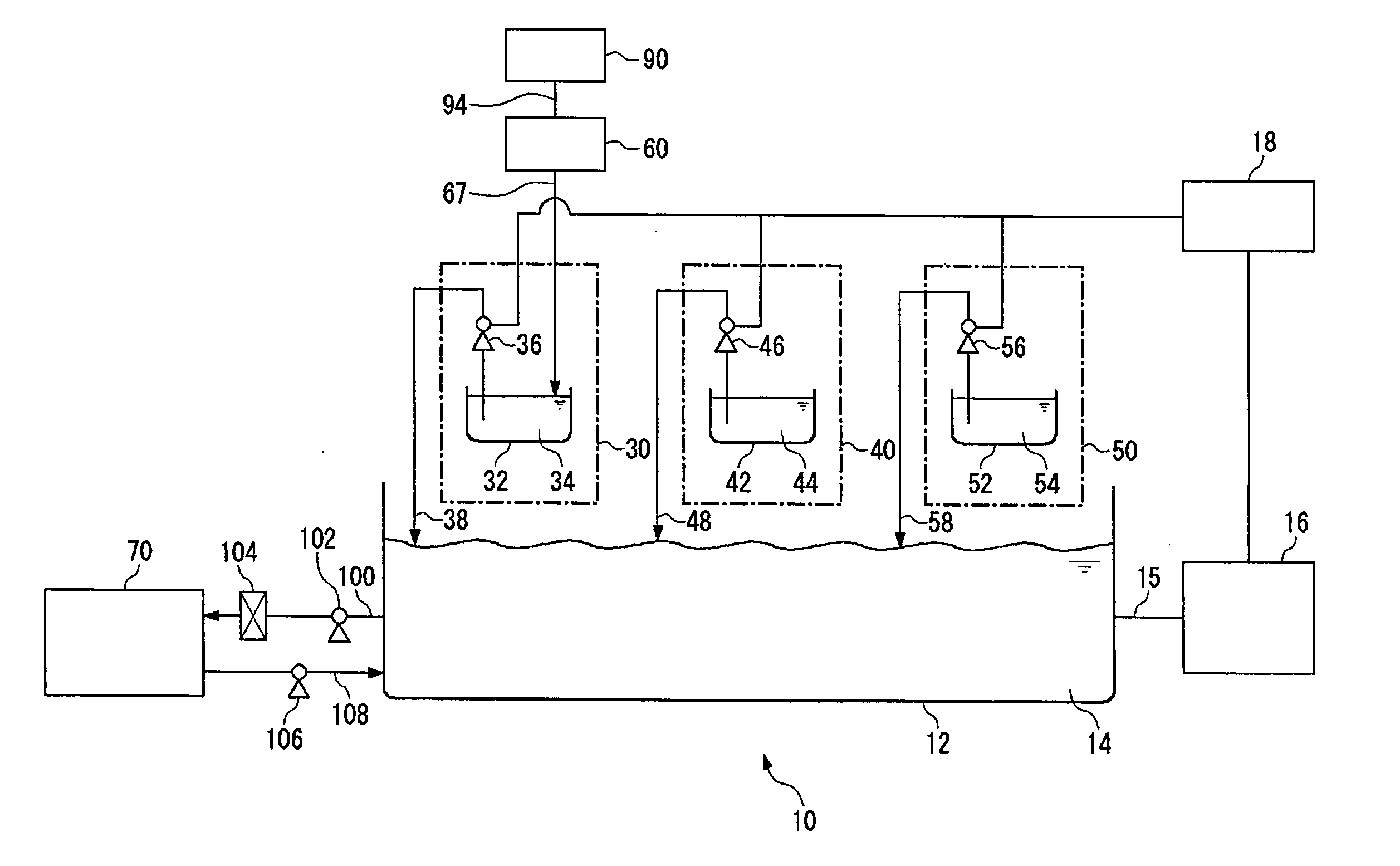
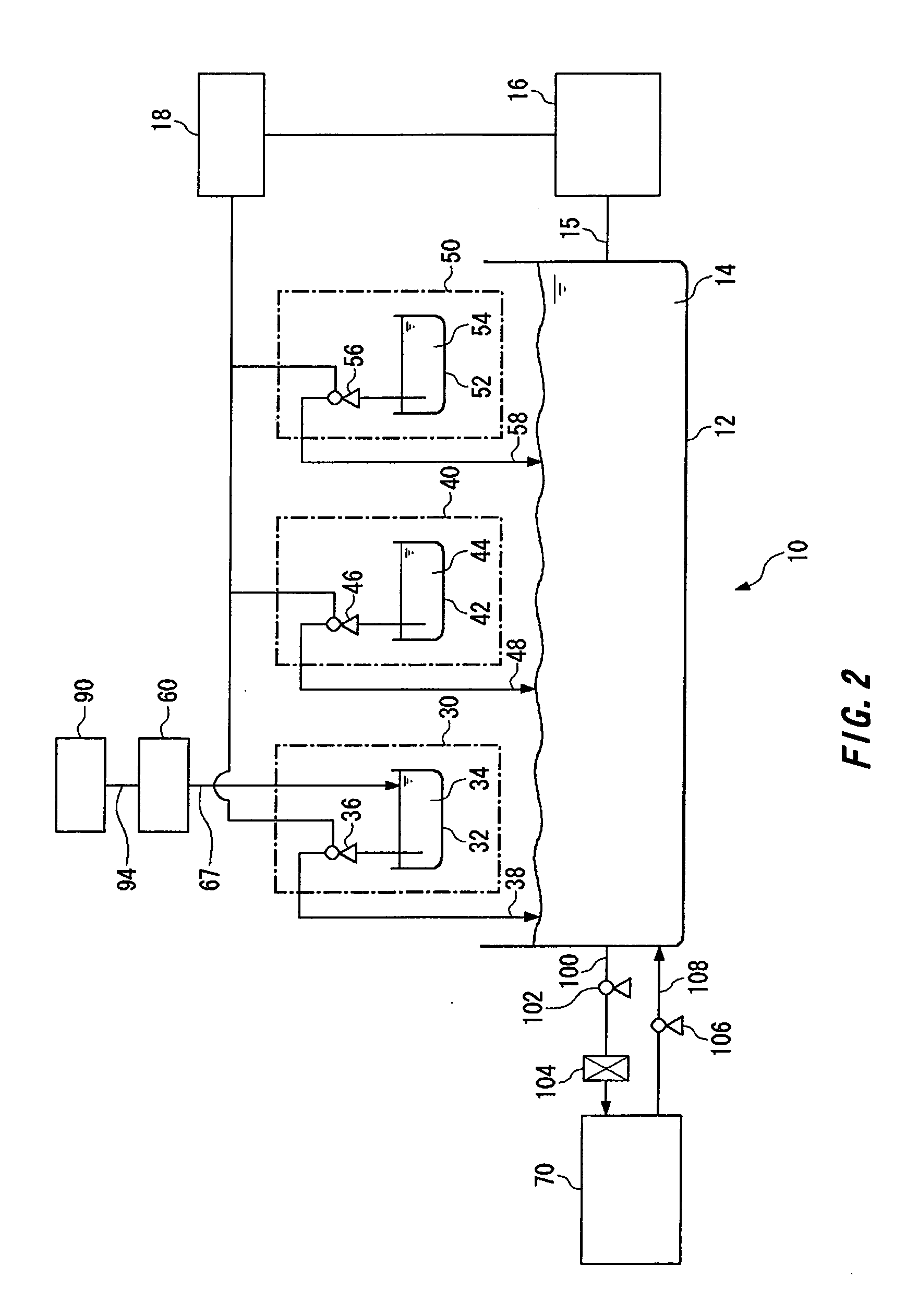
A copper plating film has a lower chlorine ion content. Circuit wiring of high electromigration resistance is formed by electroplating. In a method of copper plating using a leveler containing a nitrogen-containing high molecular compound, the leveler is dechlorinated prior to its use for plating. A plating apparatus has a tank for preparing a plating solution, a device for dechlorinating a leveler, a leveler supply station for supplying the dechlorinated leveler to the tank and a plating station. A method of forming fine circuit wiring includes forming a circuit with a phosphorus-doped copper plating layer on a substrate for an electronic circuit having a fine circuit pattern, a barrier layer and any necessary seed layer formed thereon.

Description

BACKGROUND OF THE INVENTION [0001] 1. Field of the Invention [0002] This invention relates to a copper plating method and more particularly to a copper plating method employing a dechlorinated leveler and the leveler and plating apparatus employed therefor. [0003] This invention relates also to a method of forming fine circuit wiring by plating on a substrate having a fine circuit pattern, such as a semiconductor or a printed wiring board, and particularly to a method of forming fine circuit wiring in which phosphorus-doped copper plating is relied upon for preventing the electromigration of the fine circuit wiring as formed, and a plating solution and a plating apparatus therefor. [0004] 2. Description of the Related Art [0005] Aluminum or an aluminum alloy has hitherto been used as a material for forming a wiring circuit on a semiconductor wafer. An improved degree of integration has, however, created a demand for a material of higher electric conductivity. Copper has drawn attent...

Claims


Application Information

Patent Timeline
Patent Type & Authority Applications(United States)
IPC IPC(8): C25D3/38C25D5/02C25D17/00C25D21/14H05K3/42
CPCC25D3/38H05K3/423C25D21/14
Inventor KUBOTA, MAKOTOSAHODA, TSUYOSHINAKADA, TSUTOMUMISHIMA, KOJIKIMIZUKA, RYOICHI
Owner EBARA CORP
Learn More