Testing of transimpedance amplifiers

a transimpedance amplifier and amplifier technology, applied in the field of optical communication system, can solve the problems of difficult to maintain a high quantum efficiency greater than 75%, difficult to test the high speed output signal at the wafer level, and achieve the effect of increasing efficiency

Active Publication Date: 2005-06-16
GLOBALFOUNDRIES US INC
View PDF1 Cites 6 Cited by
  • Summary
  • Abstract
  • Description
  • Claims
  • Application Information

AI Technical Summary

Benefits of technology

[0023] In accordance with the various exemplary embodiments of this invention, the small auxiliary photodete

Problems solved by technology

Given the large absorption length of silicon at a wavelength of 0.85 um, and since silicon is not sensitive to the single-mode fiber wavelengths of 1.3 um and 1.55 um, it is extremely difficult for a silicon photodetector to meet all of the requirements for operating in an optical link.
For example, since all CMOS and bipolar processes fabricate the active devices very close to the semiconductor surface, such as within 1.0 um, it is difficult to maintain a high quantum efficiency of greater than 7

Method used


Image

  • Testing of transimpedance amplifiers
  • Testing of transimpedance amplifiers
  • Testing of transimpedance amplifiers

Examples


Embodiment Construction

[0038] The following description details how exemplary aspects of the present invention are employed. Throughout the description of the invention, reference is made to FIGS. 3-10. When referring to the figures, like structures and elements shown throughout are indicated with like reference numerals.

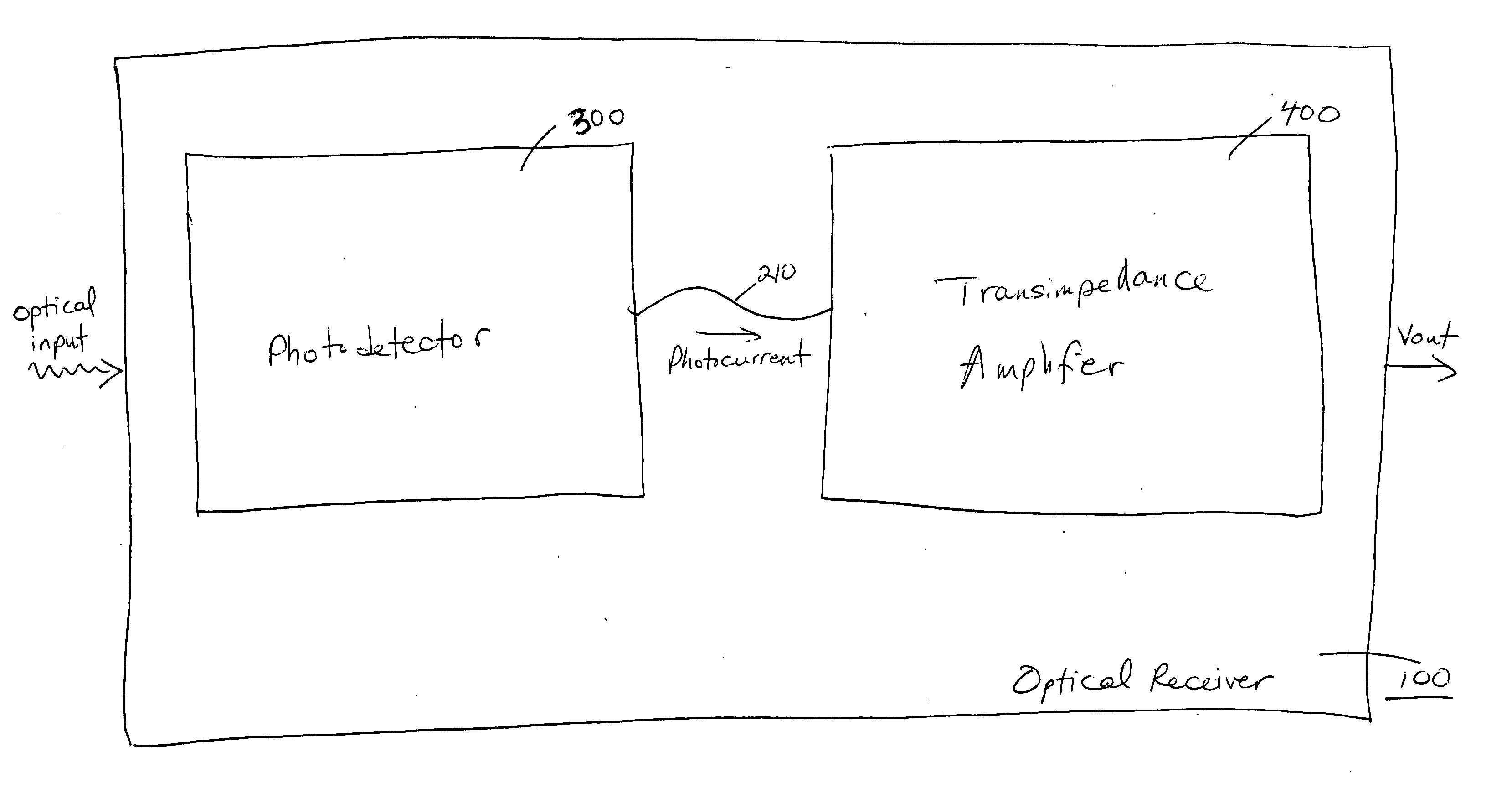
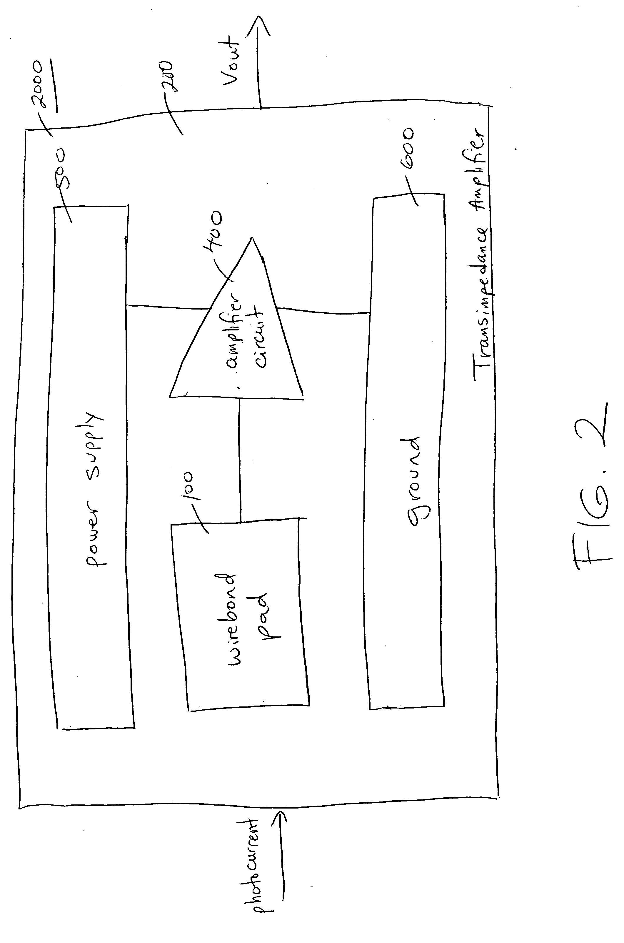
[0039] In FIG. 3, an exemplary transimpedance amplifier embodying the exemplary aspects of the present invention is shown. As shown in FIG. 3, an amplifier circuit 400 is fabricated on the substrate 200 of the transimpedance amplifier 3000 along with power supply 500 and ground 600. As shown in FIG. 3, the transimpedance amplifier 3000 further comprises an on-chip power decoupling capacitor 510 which provides high frequency currents to the amplifier circuit 400 in addition to the high frequency currents provided from external sources, and a photodetector wiring bond pad 100 for wirebonds or flip-chip attachment to an external photodetector after fabrication. Further, in accordance with a...


PUM


Abstract

Testing is performed on an amplifier wafer housing a transimpedance amplifier prior to packaging the transimpedance amplifier with an external photodetector, wherein the transimpedance amplifier includes a small, auxiliary, integrated silicon photodetector provided at the input of the transimpedance, in parallel with external photodetector attachment points. The small auxiliary photodetector does not significantly affect the high speed performance of the transimpedance amplifier. The small auxiliary photodetector is provided to facilitate wafer-level testing at the transimpedance amplifier input. To test the transimpedance amplifier, the transimpedance amplifier is stimulated by optically exciting the small auxiliary photodetector, wherein the small auxiliary photodetector is excited using short wavelength light, whereby advantages such as higher efficiency may be obtained. The testing method includes placing the amplifier wafer in a testing system, probing the power and ground connections on the amplifier wafer, illuminating the small auxiliary photodetector on the amplifier wafer, and detecting the output of the transimpedance amplifier housed on the amplifier wafer. The output of the transimpedance amplifier may detected by probing the supply voltage and detecting the switching currents passing through a bias tee using a spectrum analyzer, using a high gain antenna and a sensitive narrow band receiver, or using a high speed electrical probe.

Description

[0001] The present invention relates generally to transimpedance amplifiers, and, more specifically, to semiconductor wafers housing the transimpedance amplifiers and wafer-level testing the transimpedance amplifiers prior to packaging the transimpedance amplifiers in optical receivers. BACKGROUND [0002] In an optical communication system, a transimpedance amplifier may be used to amplify an electrical current and convert the electrical current into a voltage. A transimpedance amplifier fabricated in silicon CMOS or bipolar technology, for example, may be provided in an optical receiver along with a photodetector. [0003]FIG. 1 shows an exemplary embodiment of an optical receiver in an optical link. As shown in FIG. 1, an optical receiver 100 may comprise of a photodetector 300, and a transimpedance amplifier 400 connected to the photodetector 300 via wirebonds210. [0004] As shown in FIG. 1, the photodetector 300 receives optical input and converts the light to a proportional photocu...

Claims


Application Information

Patent Timeline
IPC IPC(8): H04B10/06H04B10/12H04B10/158
CPCH04B10/25
Inventor GUCKENBERGER, JOHN ANDREWKWARK, YOUNG HOONSCHAUB, JEREMY DANIEL
Owner GLOBALFOUNDRIES US INC
Why Eureka
Try Eureka