

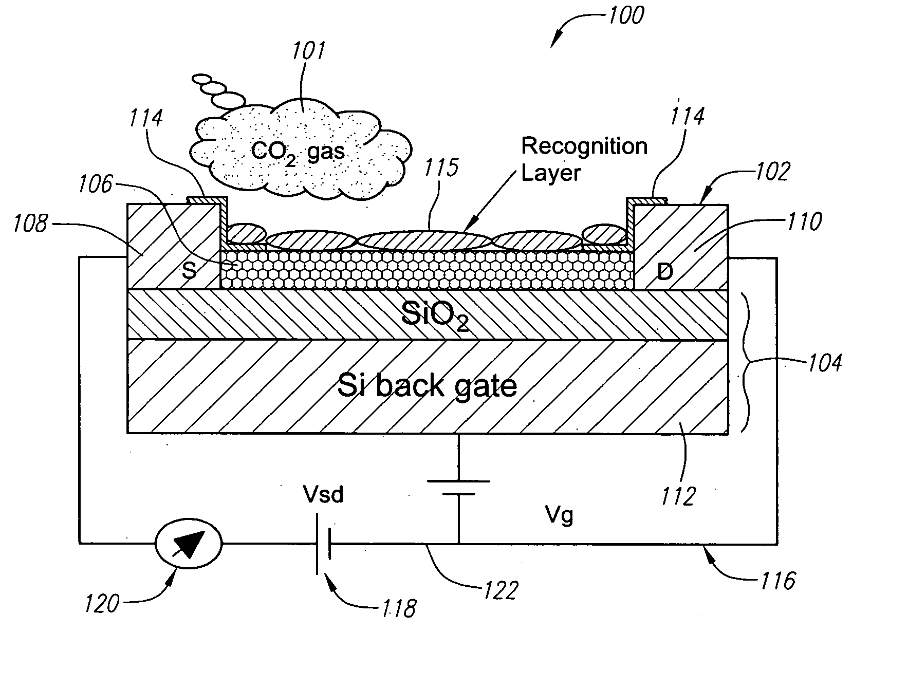
Carbon dioxide nanoelectronic sensor
a carbon dioxide and nanoelectronic technology, applied in the field of nanostructure devices, can solve the problems of limited use of these sensors, limited current technology in many ways, and limited use of cosub>2 /sub>sensors, and achieve the effect of being easily processed
- Summary
- Abstract
- Description
- Claims
- Application Information
AI Technical Summary
Benefits of technology
Problems solved by technology
Method used
Image

Examples
examples
[0036] A mixture of poly(ethylene imine) (PEI) and starch polymers as diagrammed in FIG. 3 was used for the CO2 selective recognition layer in nanotube field-effect transistor (NTFET) and nanotube network field-effect transistor (NTNFET) sensor devices. PEI, a highly branched polymer with 25% primary, 50% secondary, and 25% tertiary amino groups, can effectively adsorb CO2 from the gas mixture. A combination of PEI and starch polymers in the CO2 recognition layer is desired. Starch, a mixture of linear component amylose and branched component amylopectin, interacts strongly with nanotubes and affects CO2 reaction with PEI amino groups.
[0037] In order to improve the required sensor characteristics, the polymer layer was optimized for sensor performance by changing the ratio of polymers, deposition conditions and resulting polymer layer thickness. Modifications in the sensor platform were also made to optimize the transducer electronic characteristics and its subsequent response to C...
PUM
| Property | Measurement | Unit |
|---|---|---|
| thick | aaaaa | aaaaa |
| conducting | aaaaa | aaaaa |
| metallic | aaaaa | aaaaa |
Abstract
Description
Claims
Application Information