Process for implementing oxygen into a silicon wafer having a region which is free of agglomerated intrinsic point defects

a technology of intrinsic point defects and oxygen, which is applied in the direction of crystal growth process, testing/measurement of semiconductor/solid-state devices, transportation and packaging, etc., can solve the problems of agglomeration of intrinsic point defects, affecting the yield potential of materials, and the number of defects in single crystal silicon form, etc., to achieve the effect of improving the gettering capability

Inactive Publication Date: 2005-06-16
MEMC ELECTONIC MATERIALS INC
View PDF62 Cites 22 Cited by
  • Summary
  • Abstract
  • Description
  • Claims
  • Application Information

AI Technical Summary

Benefits of technology

[0010] Among the objects of the present invention, therefore, is the provision of a silicon on insulator structure having a device layer containing an axially symmetric region of substantial radial width which is substantially free of defects resulting from an agglomeration of crystal lattice vacancies or silicon self-interstitials; the provision of such a structure having a handle wafer with improved gettering capabilities; the provision of such a structure wherein the handle wafer comprises a silicon wafer which is capable, during the heat treatment cycles of essentially any arbitrary electronic device manufacturing process, of forming an ideal, non-uniform depth distribution of oxygen precipitates; and, the provision of such a structure which is less susceptible to the formation of metal precipitate defects during device fabrication.

Problems solved by technology

In recent years, it has been recognized that a number of defects in single crystal silicon form during the growth process as the crystal cools after solidification.
Agglomerated intrinsic point defects in silicon can severely impact the yield potential of the material in the production of complex and highly integrated circuits, such as those utilizing SOI structures.
In addition to the above-mentioned vacancy-type defects, it is also believed that agglomerated vacancy defects, or voids, may be the cause of “HF defects” (i.e., metal precipitation defects).
HF defects are, like these other vacancy-type defects, considered to be a critical problem with current SOI technology.
Such defects are not responsible for gate oxide integrity failures, an important wafer performance criterion, but they are widely recognized to be the cause of other types of device failures usually associated with current leakage problems.
Agglomerated intrinsic point defects can create performance problems for SOI substrates if silicon wafers containing such defects are utilized as the source of the device layer.
Performance problems may also result from metallic contaminants present in the handle wafer portion of the SOI structure.
This precipitation acts to disrupt the oxide layer and interfere with the performance of the SOI device.

Method used


Image

  • Process for implementing oxygen into a silicon wafer having a region which is free of agglomerated intrinsic point defects
  • Process for implementing oxygen into a silicon wafer having a region which is free of agglomerated intrinsic point defects
  • Process for implementing oxygen into a silicon wafer having a region which is free of agglomerated intrinsic point defects

Examples


example 1

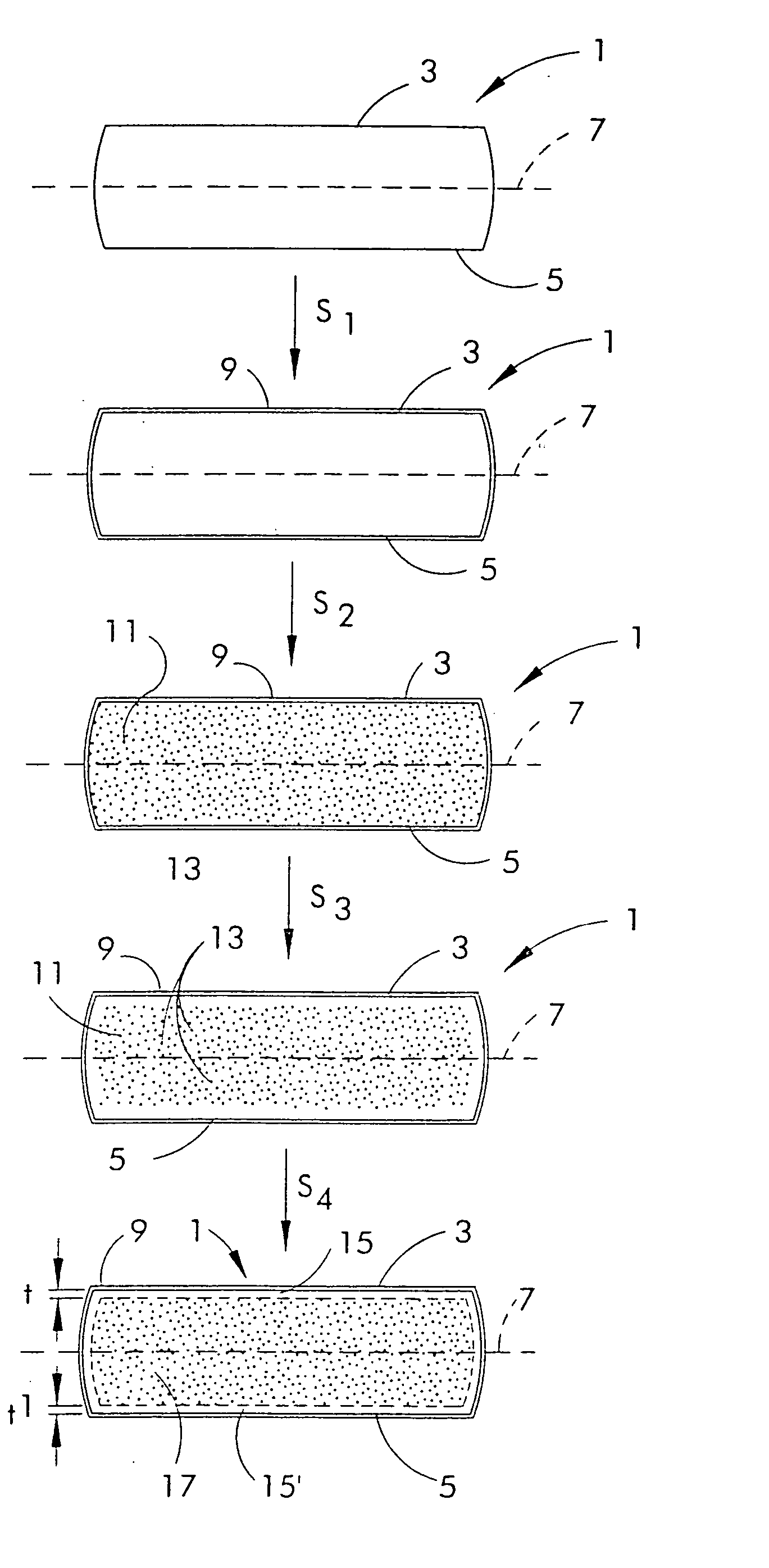
[0133] Silicon single crystals were pulled by the Czochralski method, sliced and polished to form silicon wafers. These wafers were then subjected to a surface oxidation step (S1), rapid thermal annealing step in nitrogen or argon (S2), rapidly cooled (S3), and subjected to an oxygen stabilization and growth step (S4) under the conditions set forth in Table I. The initial oxygen concentration of the wafers (Oi) before steps S1-S4, the oxygen precipitate density in the bulk of the wafers after step S4 (OPD), and the depth of the denuded zone after step S4 (DZ) are also reported in Table I.

TABLE ISample4-74-83-14S115 min at15 min atnone1,000° C.1,000° C.in N2 + ˜1%in N2 + ˜1%O2O2S235 seconds35 seconds35 secondsat 1250° C.at 1250° C.at 1250° C.in N2in Arin N2S3100° C. / sec100° C. / sec100° C. / secS44 hr at4 hr at4 hr at800° C. + 16 hr800° C. + 16 hr800° C. + 16 hratatat1,000° C.1,000° C.1,000° C.in N2in N2in N2Oi7 × 10176.67 × 1017 7.2 × 10¹⁷(atoms / cm3)OPD1 × 1010 4.4 × 1091.69 × 1010(at...

example 2

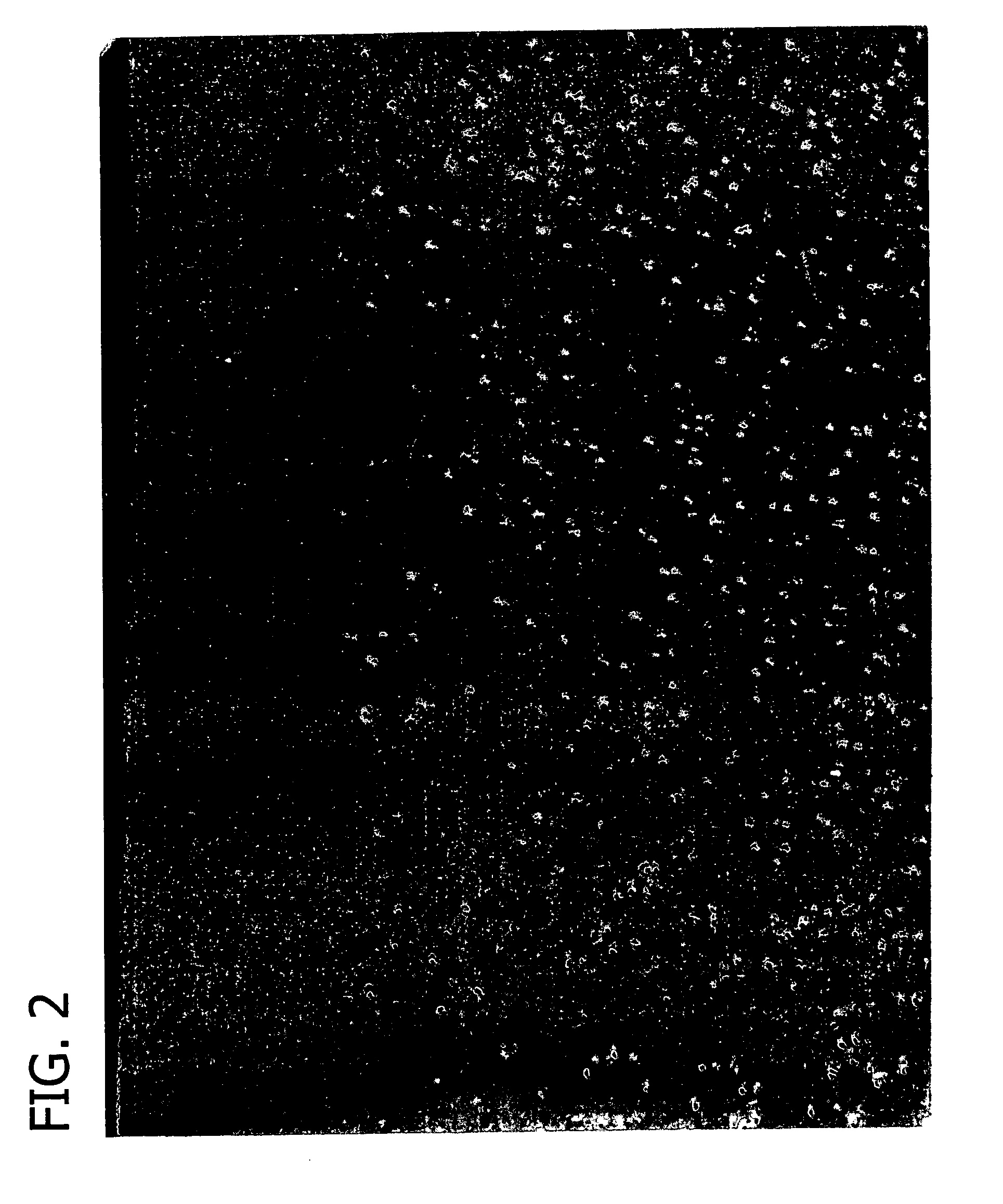
[0136] To demonstrate that the process of the present invention is relatively independent of oxygen concentration for Czochralski-grown silicon wafers, three wafers having different oxygen concentrations were subjected to the same series of steps described in Example 1. The conditions for each of these steps, the initial oxygen concentration of the wafers (Oi) before steps S1-S4, the oxygen precipitate density (OPD) in the bulk of the wafers after step S4, and the depth of the denuded zone (DZ) after step S4 as measured from the surface of the wafer are reported in Table II. FIGS. 6, 7, and 8 show cross-sections of the resulting wafers (these figures are enlargements of photographs taken at a magnification of 200×); sample 3-4 is shown in FIG. 6, sample 3-5 is shown in FIG. 7, and sample 3-6 is shown in FIG. 8.

TABLE IISample3-43-53-6S115 min at15 min at15 min at1,000° C.1,000° C.1,000° C.in N2 + ˜1%in N2 + ˜1%in N2 + ˜1%O2O2O2S235 seconds35 seconds35 secondsat 1250° C.at 1250° C.a...

example 3

[0137] To demonstrate that the process of the present invention was relatively independent of the conditions used for the oxygen precipitate stabilization and growth step (S4), a wafer (sample 1-8) having the same initial oxygen concentration was subjected to the same series of steps described in Example 2 for sample 3-4 except that a proprietary, commercial 16 Mb DRAM process was used as the oxygen precipitate stabilization and growth step (S4). FIG. 9 shows a cross-section of the resulting wafer (this figure is an enlargement of a photograph taken at a magnification of 200×). After step S4, samples 1-8 and 3-4 had comparable bulk oxygen precipitate densities (7×10¹⁰ / cm3 for sample 1-8 versus 4×10¹⁰ / cm3 for sample 3-4) and comparable denuded zone depths (approximately 40 micrometers).


PUM

PropertyMeasurementUnit
widthaaaaaaaaaa
temperatureaaaaaaaaaa
thickaaaaaaaaaa

Abstract

The present invention relates to a process for the preparation of a silicon on insulator wafer. The process includes implanting oxygen into a single crystal silicon wafer which is substantially free of agglomerated vacancy-type defects. The present invention further relates to a process for the preparation of a silicon on insulator wafer wherein oxygen is implanted into a single crystal silicon wafer having an axially symmetric region in which there is a predominant intrinsic point defect which is substantially free of agglomerated intrinsic point defects. Additionally, the present invention relates to a silicon on insulator (“SOI”) structure in which the device layer is substantially free of agglomerated intrinsic point defects.

Description

CROSS-REFERENCE TO RELATED APPLICATION [0001] This application-claims priority from U.S. application Ser. No. 10 / 038,084 filed on Jan. 3, 2002, U.S. application Ser. No. 09 / 737,715 filed on Dec. 15, 2000, which issued on Jan. 29, 2002 as U.S. Patent No. 6,342,725, U.S. application Ser. No. 09 / 387,288 filed on Aug. 31, 1999, which issued on May 22, 2001 as U.S. Pat. No. 6,236,104, and U.S. provisional application Ser. No. 60 / 098,902 filed on Sep. 2, 1998, the entire disclosures of which are incorporated herein by reference.BACKGROUND OF THE INVENTION [0002] The present invention is directed to a silicon on insulator (SOI) structure having a low defect density device layer. More specifically, the present invention is directed to a SOI structure wherein the device layer is derived from a single crystal silicon wafer which is substantially free of agglomerated intrinsic point defects. Additionally, the present invention is directed to a SOI structure having a single crystal silicon hand...

Claims


Application Information

Patent Timeline
Patent Type & Authority Applications(United States)
IPC IPC(8): C30B15/00H01L21/02H01L21/322H01L21/762H01L27/12
CPCC30B15/203C30B15/206C30B29/06H01L21/3225Y10T428/21H01L21/7624H01L21/76251Y10S257/913H01L21/3226H01L21/76254
Inventor FALSTER, ROBERT J.
Owner MEMC ELECTONIC MATERIALS INC
Why Eureka
Try Eureka