Circuits, multilayer circuits, and method of manufacture thereof

Active Publication Date: 2005-06-23
WORLD PROPERTIES
View PDF40 Cites 10 Cited by
  • Summary
  • Abstract
  • Description
  • Claims
  • Application Information

AI Technical Summary

Benefits of technology

[0013] The above-described drawbacks and disadvantages are alleviated by a method for the manufacture of a multilayer circuit comprising a liquid crystalline polymer layer, the method comprising treating the multilayer circuit with an amount of heat effective to raise the crystalline to nematic melting point, as defined by the peak endotherm above the glass transition temperature in a differen

Problems solved by technology

Canadian Patent Application No. 2,273,542 to Forcier, for example, describes a circuit laminate made by bonding an adhesive resin-coated copper foil to a thin liquid crystal polymer film, but does not disclose how to make these circuit laminates into multilayer circuits.
While a variety of materials and methods are known for producing multilayer circuits using liquid crystalline polymers, including annealed liquid crystalline polymers, they suffer from a number of drawbacks that limit their utility.
When current commercially available liquid crystalline polymers are used as bond plies, the bond plies re-melt upon soldering or ot

Method used


Image

  • Circuits, multilayer circuits, and method of manufacture thereof
  • Circuits, multilayer circuits, and method of manufacture thereof
  • Circuits, multilayer circuits, and method of manufacture thereof

Examples


example 1

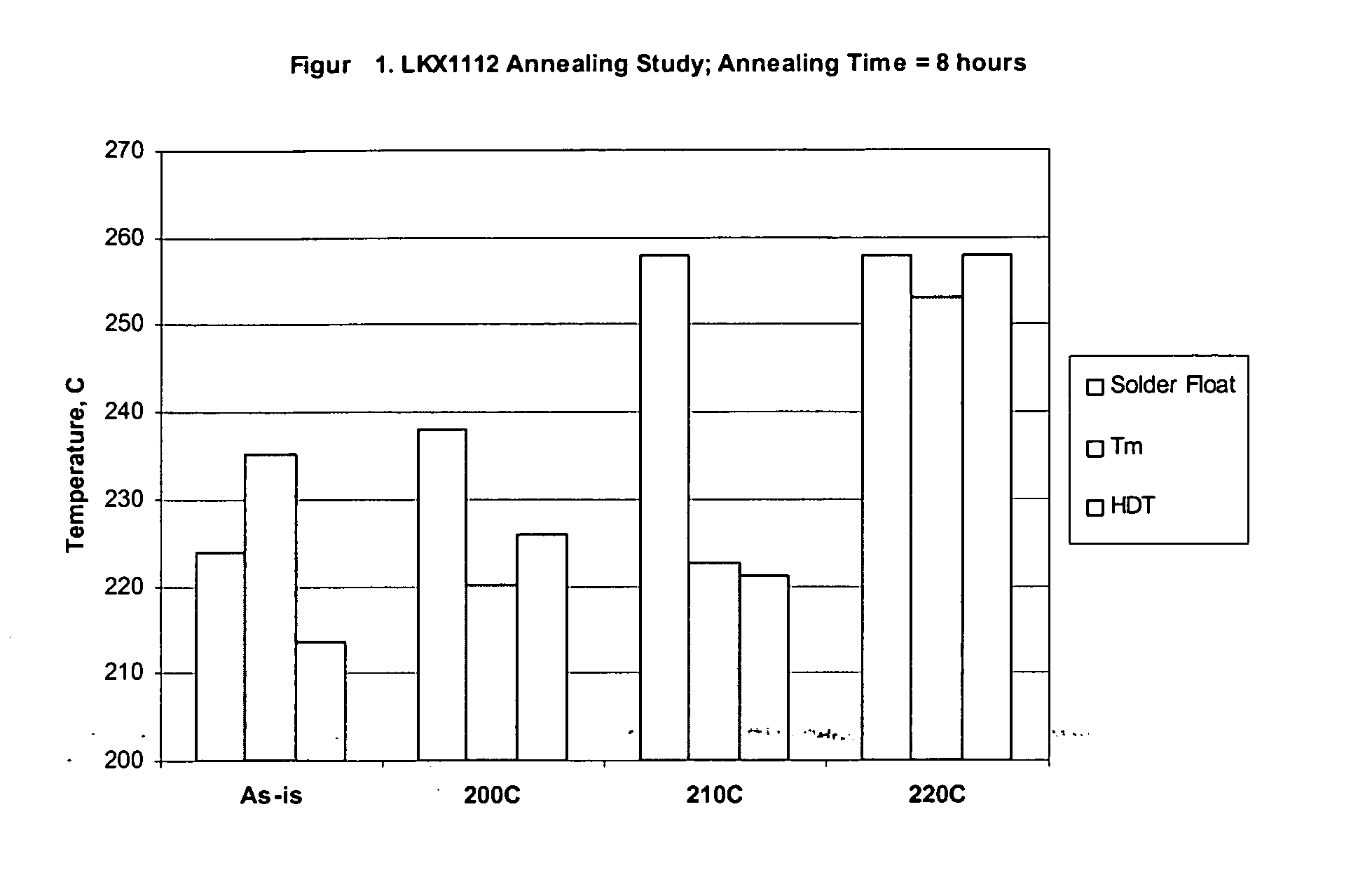
Increasing the temperature resistance of Vectra LKX 1112 Liquid Crystalline Polymer Bond Ply

[0060] To demonstrate the increase in practical multi-layer circuit properties that are achievable with a post-lamination annealing step, the following experiment was conducted. Two sheets of 17-micrometer thick NT-TOR copper foil (manufactured by Circuit Foils Luxembourg) were laminated together with a 50-micrometer thick sheet of liquid crystalline polymer bond ply Vectra® LKX1112 liquid crystalline polymer (Ticona Corporation). Vectra® LKX1112 liquid crystalline polymer exhibits a melting point (as measured by the peak value of the melting point by differential scanning calorimetry (DSC)) of 232° C. The press temperature program began with the press pre-heated to 95° C., increasing the temperature to 230° C. at a rate of 3.3° C. / minute and a pressure of 400 psi), holding the press for 15 minutes at 230° C., and then cooling the press to room temperature at a rate of 3.3° C. / minute.

[0061]...

example 2

Multiple Sequential Multi-Layer Laminations with Rogers R / Flex 3800 LCPfilm.

[0066] The following example demonstrates sequential lamination using liquid crystalline polymer resin coated conductive foils and the improvement in the method achieved by annealing the multi-layer circuit subassemblies after lamination.

[0067] A circuit comprising Rogers R / flex 3800 liquid crystalline polymer film as the dielectric layer, and which is clad on both sides with copper foil is available from Rogers Corporation under the trade name R / flex 3850®. The liquid crystalline polymer circuit substrate in this material exhibits a nematic melting point as measured by DSC of 315° C. A circuit substrate having a Rogers R / flex 3800 liquid crystalline polymer film as the dielectric layer, and which is clad on one side with copper foil is available from Rogers Corporation under the trade name R / flex 3600®. The liquid crystalline polymer substrate in this material exhibits a nematic melting point of 290° C. a...


PUM

PropertyMeasurementUnit
Temperatureaaaaaaaaaa

Abstract

A method for the manufacture of a multilayer circuit comprising a liquid crystalline polymer layer, the method comprising treating the multilayer circuit with an amount of heat effective to raise the crystalline to nematic melting point, as defined by the peak endotherm above the glass transition temperature in a differential scanning calorimeter measurement, of the liquid crystalline polymer layer by at least about 10° C.

Description

BACKGROUND [0001] This invention relates to multilayer circuits comprising liquid crystalline polymers (LCPs) and methods for the manufacture thereof. [0002] As used herein, a circuit material is an article used in the manufacture of circuits and multilayer circuits, and includes circuit laminates, bond plies, conductive layers, resin coated conductive layers, and cover films. These circuit materials each comprise dielectric materials formed from a thermosetting or thermoplastic polymer. The dielectric material in a bond ply, resin covered conductive layer, or cover film may comprise a substantially non-flowable dielectric material, i.e., one that softens or flows during manufacture but not during use of the circuit. The dielectric material in a circuit laminate (i.e., a dielectric substrate), in contrast, is designed to not soften or flow during manufacture or use of the circuit or multi-layer circuit. Dielectric substrate materials are further typically divided into two classes, f...

Claims


Application Information

Patent Timeline
IPC IPC(8): H05K1/03H05K3/00H05K3/46
CPCH05K3/0011H05K3/4626H05K2201/0141Y10T29/49128Y10T29/49126Y10T29/49124Y10T29/49155H05K2203/1105
Inventor ROSEEN, E. CLIFFORD JR.KENNEDY, SCOTT D.HAND, DORIS I.WHITE, MICHAEL S.HORN, ALLEN F. III
Owner WORLD PROPERTIES
Why Eureka
Try Eureka