Silicon solar cell and production method thereof

Inactive Publication Date: 2005-06-23
HITACHI LTD
View PDF7 Cites 184 Cited by
  • Summary
  • Abstract
  • Description
  • Claims
  • Application Information

AI Technical Summary

Benefits of technology

[0005] A silicon solar cell with n+pp+ structure produced by phosphorus and boron diffusion by a conventional technique, is contaminated with Fe not only in the silicon substrate manufacturing process but also in cell production steps. At the same time, treating p-type silicon by boron diffusion reduces its bul

Problems solved by technology

A silicon solar cell with n+pp+ structure produced by phosphorus and boron diffusion by a conventional technique, is contaminated with Fe not only in the silicon substrate manufacturing process but also in cell production steps.
At the same time, treating p-type silicon by boron diffusion reduces its bulk effective life time to around 10 μs, making it difficult to secure sufficient cell performance, because the reduced life time is recovered to a limited extent by phosphorus gettering alone, which accompanies phosphorus diffusion.
Moreover, heat treatment in the electrode firing step also reduces its life time.
A glass-glass module using conventional mono-facial cells has a disadvantage related to outer appearances for the

Method used


Image

  • Silicon solar cell and production method thereof
  • Silicon solar cell and production method thereof
  • Silicon solar cell and production method thereof

Examples


Example

EXAMPLE 1

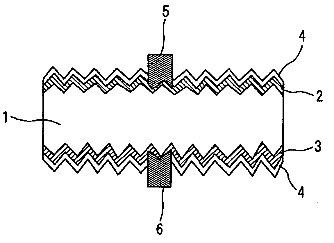
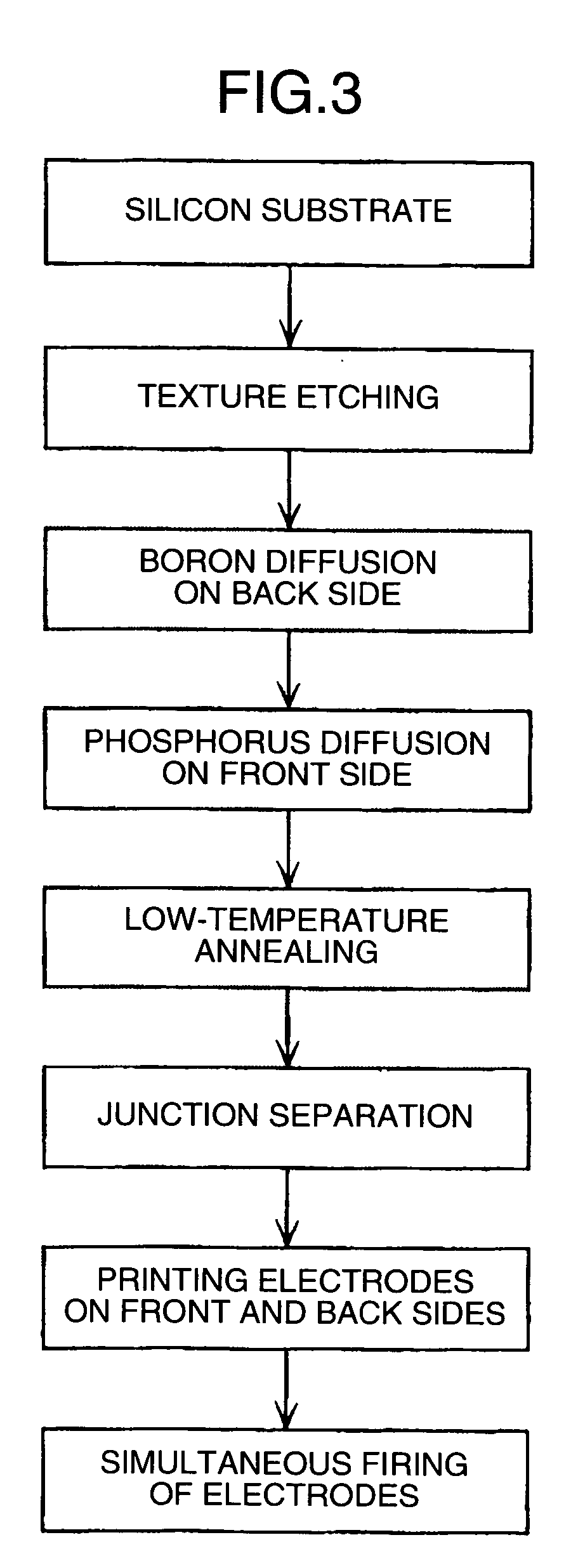
[0032]FIG. 1 illustrates a cross-sectional structure of the solar cell produced in Example 1, where the silicon substrate 1 may be of p- or n-type. The solar cell is described here taking a p-type substrate as an example.

[0033] The solar cell of Example 1 comprises the silicon substrate 1 coated with the n+ layer 2 on the front side and p+ layer 3 on the back side, the former being formed by phosphorus diffusion and the latter by boron diffusion, where the n+ layer 2 and p layer of the silicon substrate 1 form the p-n junction while the p+ layer 3 forms a BSF. Each of the n+ layer 2 and p+ layer 3 is coated with the silicon oxide (SiO2) film 4.

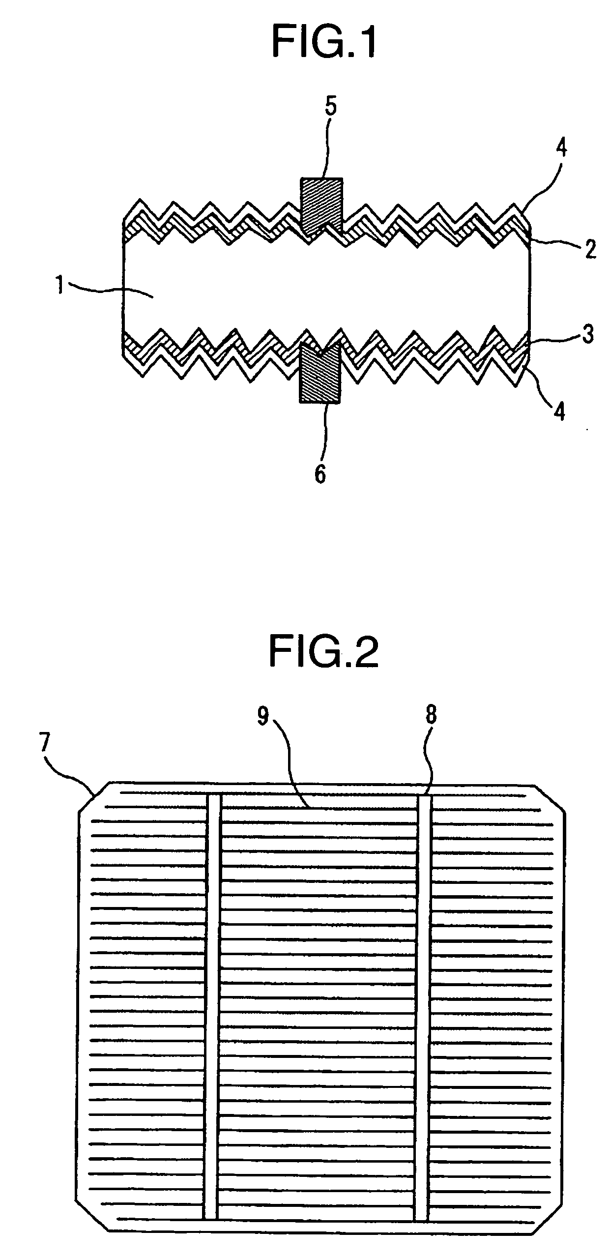
[0034] The n+pp+-diffused substrate of BSF structure is coated with the respective front electrode 5 as the cathode on the front side and back electrode 6 as the anode on the back side. The grid-shape electrode for the silicon solar cell of Example 1 is composed of the busbar electrodes 8 and finger electrodes 9, as illustrated in ...

Example

EXAMPLE 2

[0046] The solar cell with n+pp+ BSF structure was produced in Example 2 in the same manner as in Example 1, except that it was coated with the grid-shape electrode, as illustrated in FIG. 2, on the front side, not expecting positive photosensitivity on the back side. Therefore, it differs from the cell produced in Example 2 only in that the electrode accounts for a larger area and is arranged more finely and tightly as shown at FIG. 5. In other words, area ratio of the grid-shape electrode on the front side to the front side surface is smaller than that of the grid-shape electrode on the back side to the back side surface.

[0047] A mono-facial cell by conventional technique, illustrated in FIG. 6, comprises the n+p-diffused substrate 12 coated with the aluminum electrode 13 of uneven brownish red color over the entire back side. By contrast, the mono-facial cell of Example 2, illustrated in FIG. 5, comprises the n+pp+-diffused substrate 7 coated with the busbar electrodes...

Example

[0049] The solar cell was produced in the same manner as in Example 1 or 2, except that the fine finger electrodes 9 (width: 100 μm or less) were made thicker at the bases 11 on the busbar electrode 8, as illustrated in FIG. 7. The width of the busbar electrode 8 in the cell of Example 3 is at least 10 times wider than that of the finger electrode 9 and is 1 to 3 mm. The wider base 11 is rectangular (FIG. 7 (A)) or triangular (FIG. 7(B)), and the finger electrodes 9 are made 2 to 4 times wider in width at a portion around 1 mm from the base 11. The width of the finger electrode 9 may be made wider in the section from the base 11 to 0.3 to 2 times of the busbar electrode width. The solar cell of Example 3 has improved cell performance, because the finger electrodes 9 for the grid-shape electrode are made finer to increase number of the finger electrodes 9 and thereby to reduce series resistance of the cell.

[0050] As discussed above, Example 3 realizes a solar cell of high efficiency...


PUM


Abstract

It is an object of the present invention to provide a silicon solar cell with n+pp+ BSF structure using solar grade silicon substrate, having a life time close to the initial level of the substrate. The solar cell of the present invention is produced by a back side boron diffusion step for diffusing boron on a back side of the substrate, a front side phosphorus diffusion step for diffusing phosphorus on a front side of the substrate, a low-temperature annealing step for annealing the substrate at 600° C. or lower for 1 hour or more, and an electrode firing step carried out at a peak temperature of 700° C. or lower for 1 minute or less, carried out in this order.

Description

FIELD OF THE INVENTION [0001] The present invention relates to a silicon photovoltaic solar cell and production method thereof. BACKGROUND OF THE INVENTION [0002] A silicon solar cell (mono-facial cell) by a conventional technique comprises a p-type silicon substrate, in which an n+ layer is formed by phosphorus diffusion and a grid-shape silver electrode in this order on the front side and with aluminum electrode over the entire back side, where these electrodes are formed by printing and firing process. More specifically, aluminum paste is printed and then fired at around 800° C., which diffuses the aluminum atoms into the silicon substrate to form the p+ layer on the back side. This p+ layer works as a back surface field (hereinafter referred to as BSF), which improves cell performance. At the same time, phosphorus gettering takes place while phosphorus is being diffused, and aluminum gettering takes place while the electrode is being fired, to improve life time of bulk silicon a...

Claims


Application Information

Patent Timeline
IPC IPC(8): H01L31/00H01L31/0224H01L31/0352H01L31/04H01L31/042H01L31/06H01L31/068H01L31/18
CPCH01L31/03529Y02E10/547H01L31/068
Inventor JOGE, TOSHIOARAKI, ICHIROHOSOYA, TOMONORI
Owner HITACHI LTD
Why Eureka
Try Eureka