High performance embedded semiconductor memory devices with multiple dimension first-level bit-lines

a semiconductor memory and embedded technology, applied in semiconductor devices, digital storage, instruments, etc., can solve the problem of no longer having tight pitch layout problems for sense amplifiers and other peripheral circuits, and achieve the effect of improving the performance of semiconductor memory devices, facilitating the integration of memory cells, and simplifying the support system

Inactive Publication Date: 2005-06-23
UNIRAM TECH
View PDF38 Cites 46 Cited by
  • Summary
  • Abstract
  • Description
  • Claims
  • Application Information

AI Technical Summary

Benefits of technology

[0013] The primary objective of this invention is, therefore, to improve the performance of semiconductor memory device without paying extensive area penalty. Another primary objective is to make DRAM user-friendlier by making the performance improvement in parallel with simplificati

Problems solved by technology

Therefore, we no longer have tight pitch layout probl

Method used


Image

  • High performance embedded semiconductor memory devices with multiple dimension first-level bit-lines
  • High performance embedded semiconductor memory devices with multiple dimension first-level bit-lines
  • High performance embedded semiconductor memory devices with multiple dimension first-level bit-lines

Examples


Embodiment Construction

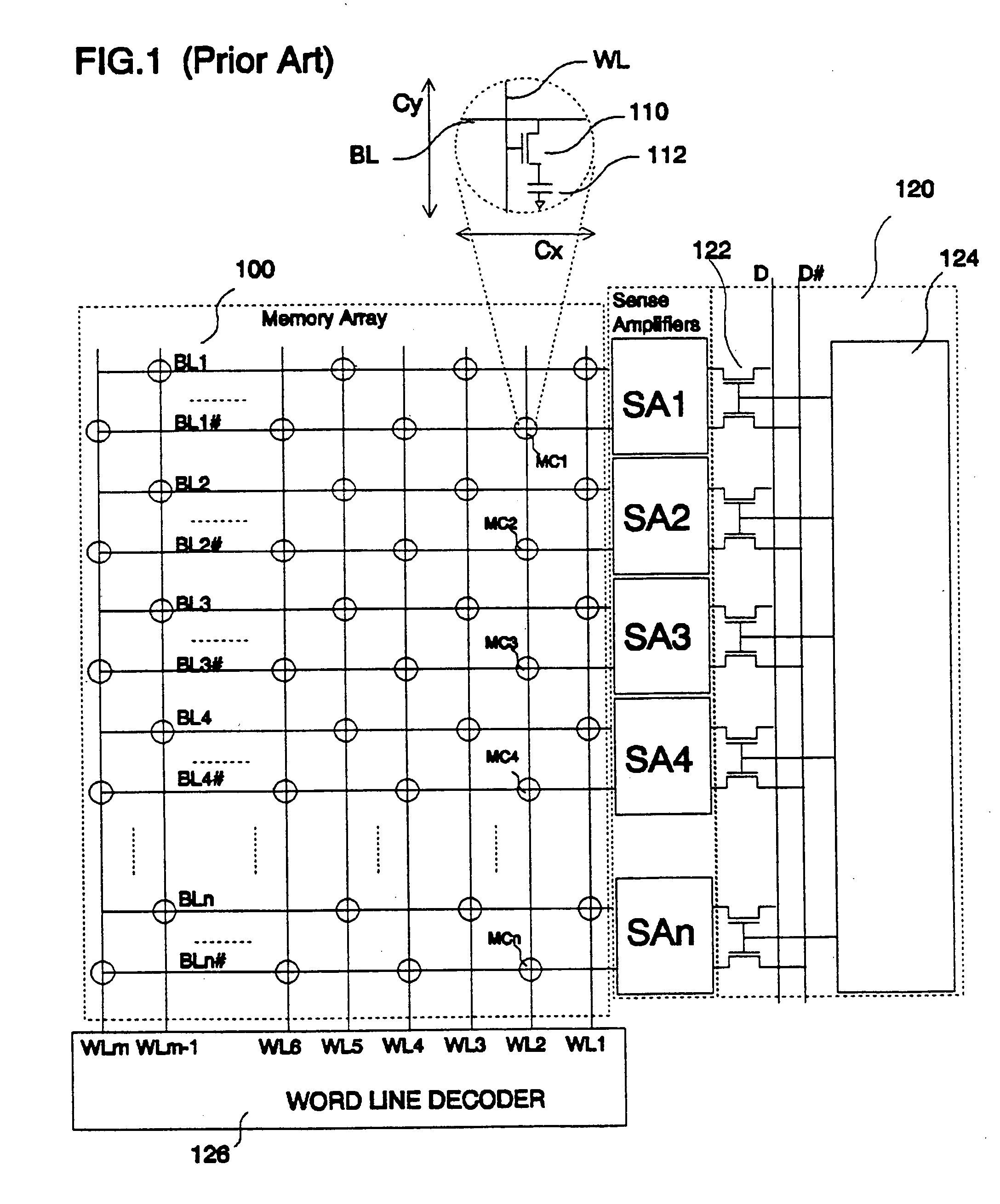
[0053] Before the invention itself is explained, a prior art semiconductor memory-device is first explained to facilitate the understanding of the invention.

[0054]FIG. 1 shows memory cell array structure of a prior art DRAM in both electrical and topographical manners. Memory cell array 100 includes plural pairs of bit lines BL1, BL1#; BL2, BL2#, BL3, BL3#; . . . ; BLn, BLn# (n; integer) which are disposed in parallel manner and a plurality of word lines WL1, WL2 . . . WLm (m; integer) which are disposed in parallel manner and also in such manner that they intersect with bit lines perpendicularly. At intersecting points, memory cells MC1, MC2, . . . , MCn are disposed. Memory cells are shown by circle marks in memory cell array 100 in FIG. 1. Each memory cell includes a switching field effect transistor 110 and memory cell capacitor 112. Bit line BL is connected to the drain of the transistor 110. The gate of transistor 110 is connected to word line WL. Sense amplifiers SA1, SA2, ....


PUM


Abstract

A dynamic random access memory solves long-existing tight pitch layout problems using a multiple-dimensional bit line structure. Improvement in decoder design further reduces total area of this memory. A novel memory access procedure provides the capability to make internal memory refresh completely invisible to external users. By use of such memory architecture, higher performance DRAM can be realized without degrading memory density. The requirements for system support are also simplified significantly.

Description

[0001] This is a Continuous Prosecution Application (CPA) of a previously filed co-pending Application with Ser. No. 10 / 269,571 filed on Oct. 10, 2002. The application Ser. No. 10 / 269,571 is a Continuation in Part Application of the application Ser. No. 09 / 860,215 and that is a Continuation in Part (CIP) Application of another application Ser. No. 08 / 653,620 filed on May 24, 1996 and another co-pending application Ser. No. 08 / 805,290 filed on Feb. 25, 1997 and an International Application filed in Taiwan Intellectual Property Bureau by identical sole inventor as for this CIP Application by identical sole inventor as for this Continuation-in-Part (CIP) Application.BACKGROUND OF THE INVENTION [0002] 1. Field of the Invention [0003] The present invention relates to high performance semiconductor memory devices, and more particularly to embedded memory devices having first level bit lines connected along different layout directions. [0004] 2. Description of the Prior Art [0005] DRAM is ...

Claims


Application Information

Patent Timeline
IPC IPC(8): G11C7/18G11C11/404G11C11/408H01L21/8238H01L27/02H01L27/105H01L27/108H01L29/788
CPCG11C7/18G11C11/404G11C11/4087G11C2207/104H01L27/10897H01L27/0214H01L27/105H01L27/10829H01L21/823857H10B12/37H10B12/50
Inventor SHAU, JENG-JYE
Owner UNIRAM TECH
Why Eureka
Try Eureka