Semiconductor device and method of manufacturing the same

a technology of semiconductor devices and semiconductors, applied in the direction of solid-state devices, transistors, inductances, etc., can solve the problems of reducing breakdown voltage, kinks, and various problems of the soi device with the fti structure, and achieve the effect of reducing the parasitic capacitance of the resistive element and high circuit performan

Inactive Publication Date: 2005-06-23
RENESAS TECH CORP
View PDF5 Cites 19 Cited by
  • Summary
  • Abstract
  • Description
  • Claims
  • Application Information

AI Technical Summary

Benefits of technology

[0017] It is an object of the present invention to form an SOI device which prevents occurrence of dishing and pro

Problems solved by technology

As such, the SOI device with the FTI structure has suffered from various problems associated with floating body effects.
For example, a kink occurs, a breakdown voltage is reduced, or a delay time becomes frequency-dependent because of unstable potential of the channel region.
To form the resistive elements on the full-t

Method used


Image

  • Semiconductor device and method of manufacturing the same
  • Semiconductor device and method of manufacturing the same
  • Semiconductor device and method of manufacturing the same

Examples


first modification

[0125] D. First Modification

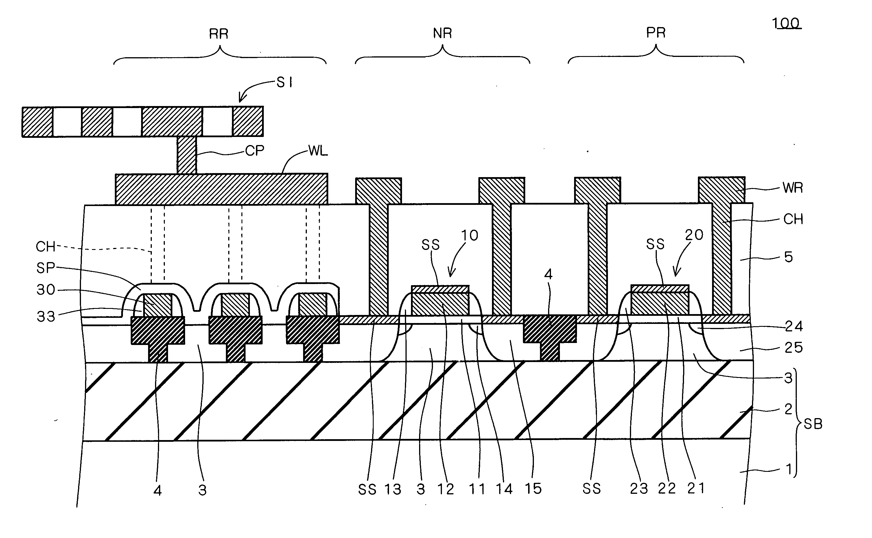
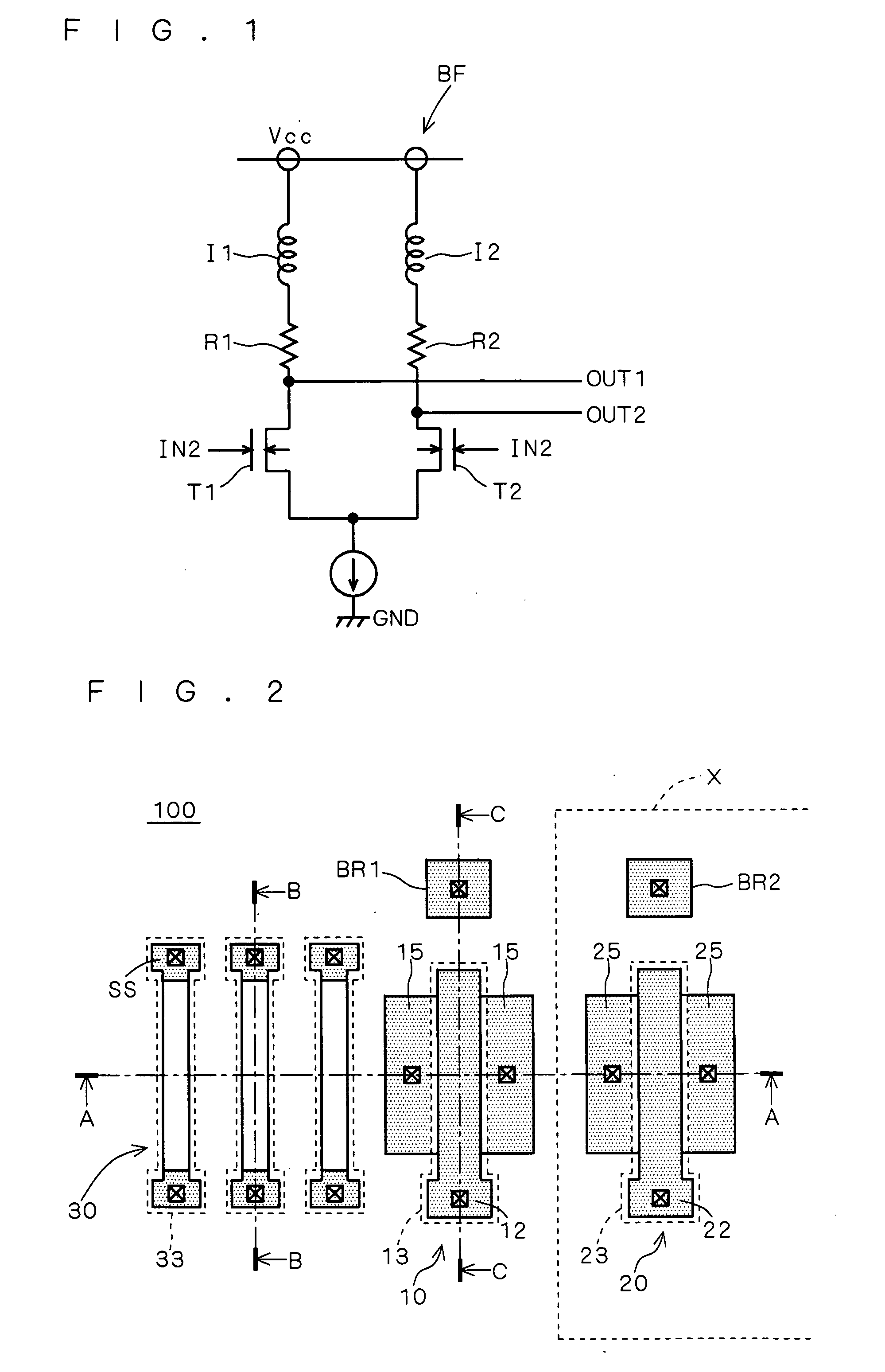
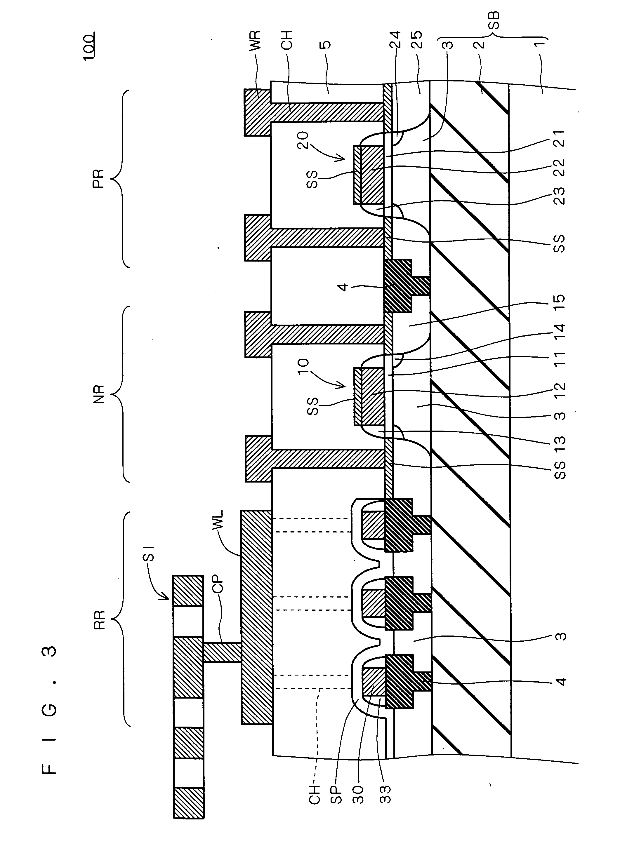
[0126] According to the above-described preferred embodiment, implantation of impurities into the SOI layer 3 is prevented in the resistor region RR during formation of the semiconductor element. By doing so, the resistance of the SOI layer 3 can be kept high in the resistor region RR, and also, the SOI layer 3 can be fully depleted in the resistor region RR, depending on a voltage. In contrast thereto, to implant impurities into the resistive elements 30 at the time of source / drain doping, for example, would allow reduction of a resistance of each of the resistive elements 30. To this end, not a resist mask including an opening which exposes the whole resistor region RR, but a resist mask including openings which expose only the resistive elements 30, respectively, in the resistor region RR, is formed so that implantation of impurities into the portions of the SOI layer 3 interposed between the trench isolation films 4 can be prevented.

[0127] In forming...

second modification

[0129] E. Second Modification

[0130] According to the above-described preferred embodiment, the trench isolation films 4 each with the hybrid-trench isolation structure are provided at intervals with portions of the SOI layer 3 interposed therebetween, and the resistive elements 30 are formed on the trench isolation films 4, respectively, in the resistor region RR. Alternatively, trench isolation films each with the full-trench isolation structure may be provided in place of the trench isolation films 4, in the resistor region RR. Below, a structure according to a second modification, which includes the trench isolation films each with the full-trench isolation structure in the resistor region RR, as well as manufacture thereof, will be described with reference to FIGS. 26, 27, 28, and 29. FIGS. 26, 27, 28 and 29 illustrate steps for manufacturing the trench isolation films according to the second modification in order of occurrence.

[0131] After the steps illustrated in FIGS. 6, 7, ...

third modification

[0137] F. Third Modification

[0138] According to the above-described preferred embodiment, implantation of impurities into the SOI layer 3 is prevented in the resistor region RR during formation of the semiconductor element. By doing so, the resistance of the SOI layer 3 can be kept high in the resistor region RR, and also the SOI layer 3 can be fully depleted in the resistor region RR, depending on a voltage. In this regard, not only the SOI layer 3 in the resistor region RR, but also the trench isolation films 4 in the resistor region RR, are not subjected to implantation of impurities. As a result, a thickness of each of the trench isolation films in the resistor region RR can be made larger than that in the element region.

[0139] Specifically, to implant impurities into the trench isolation films would increase an etching rate in hydrofluoric acid (HF) etching which is to be later performed for removing the silicon oxide film.

[0140] For example, as described above with reference...


PUM


Abstract

Plural trench isolation films (4) are provided with portions of an SOI layer (3) interposed therebetween in a surface of the SOI layer (3) in a resistor region (RR) where a spiral inductor (SI) is to be provided. Resistive element (30) are formed on the trench isolation films (4), respectively. Each of the trench isolation films (4) includes a central portion which passes through the SOI layer (3) and reaches a buried oxide film (2) to include a full-trench isolation structure, and opposite side portions each of which passes through only a portion of the SOI layer (3) and is located on the SOI layer 3 to include a partial-trench isolation structure. Thus, each of the trench isolation films (4) includes a hybrid-trench isolation structure.

Description

BACKGROUND OF THE INVENTION [0001] 1. Field of the Invention [0002] The present invention relates to a semiconductor device and a method of manufacturing the same, and more particularly to a semiconductor device including an inductor and a method of manufacturing the same. [0003] 2. Description of the Background Art [0004] A semiconductor device formed on an silicon-on-insulator (SOI) substrate which includes a buried oxide film and an SOI layer deposited on a silicon substrate (such semiconductor device will be hereinafter referred to as an “SOI device”) is characterized by a lower parasitic capacitance, a high-speed and reliable operation, and lower power consumption, and is used in a portable equipment or the like. [0005] One example of an SOI device is an SOI device with a “full-trench isolation (FTI) structure”. In SOI device with the FTI structure, a trench reaching a buried oxide film is formed in a surface of an SOI layer and is filled with an insulator (which will hereinaft...

Claims


Application Information

Patent Timeline
IPC IPC(8): H01L21/76H01L21/762H01L21/822H01L21/8234H01L21/84H01L27/04H01L27/06H01L27/08H01L27/12H01L27/13H01L29/786
CPCH01L21/76283H01L21/84H01L27/0617H01L27/0629H01L27/1203H01L29/7833H01L28/10H01L28/20H01L29/665H01L29/6659H01L27/13H01L27/04
Inventor IWAMATSU, TOSHIAKIIPPOSHI, TAKASHI
Owner RENESAS TECH CORP
Why Eureka
Try Eureka