Laser irradiation method and method for manufacturing crystalline semiconductor film

a technology of crystalline semiconductor and laser irradiation, which is applied in the direction of manufacturing tools, instruments, and therapy, can solve the problems of homogeneous energy given to the irradiated object, and achieve the effect of suppressing the inhomogeneity of irradiation energy

Active Publication Date: 2005-06-30
SEMICON ENERGY LAB CO LTD
View PDF33 Cites 45 Cited by
  • Summary
  • Abstract
  • Description
  • Claims
  • Application Information

AI Technical Summary

Benefits of technology

[0009] Consequently, the present invention is made in view of the above problem, and it is an object of the present invention to provide a laser irradiation method that can suppress the inhomogeneity of the irradiation energy on the irradiated surface.
[0010] Moreover, it is another object of the present invention to provide a method for manufacturing a crystalline semiconductor film whose crystallinity is more homogeneous.
[0019] The present invention discloses another method for manufacturing a crystalline semiconductor film comprises irradiating a crystalline semiconductor film formed over a substrate having a refractive index n and a thickness d with a laser beam emitted from a pulsed laser oscillator so as to improve crystallinity of the crystalline semiconductor film, and a pulse width t of the laser beam satisfies an inequality ct<2nd where c is a speed of light in vacuum.
[0020] The present invention discloses another method for manufacturing a crystalline semiconductor film comprises irradiating a crystalline semiconductor film formed over a substrate having a refractive index n and a thickness d with a laser beam emitted from a pulsed laser oscillator so as to improve crystallinity of the crystalline semiconductor film, and a pulse width t of the laser beam satisfies an inequality ct<4nd where c is a speed of light in vacuum.
[0024] When the method for manufacturing a crystalline semiconductor film of the present invention is applied to manufacture a crystalline semiconductor film, it is possible to crystallize the irradiated object homogeneously at high throughput and therefore to obtain a crystalline semiconductor film having superior characteristic. Moreover, when semiconductor elements are manufactured using the crystalline semiconductor film that is crystallized by the present invention, the variation of the characteristic can be reduced between the semiconductor elements.

Problems solved by technology

However, even when the laser irradiation is performed under the same condition after adjusting the energy distribution of the beam spot as appropriate, the energy given to the irradiated object is not homogeneous yet.

Method used


Image

  • Laser irradiation method and method for manufacturing crystalline semiconductor film
  • Laser irradiation method and method for manufacturing crystalline semiconductor film
  • Laser irradiation method and method for manufacturing crystalline semiconductor film

Examples


embodiment 1

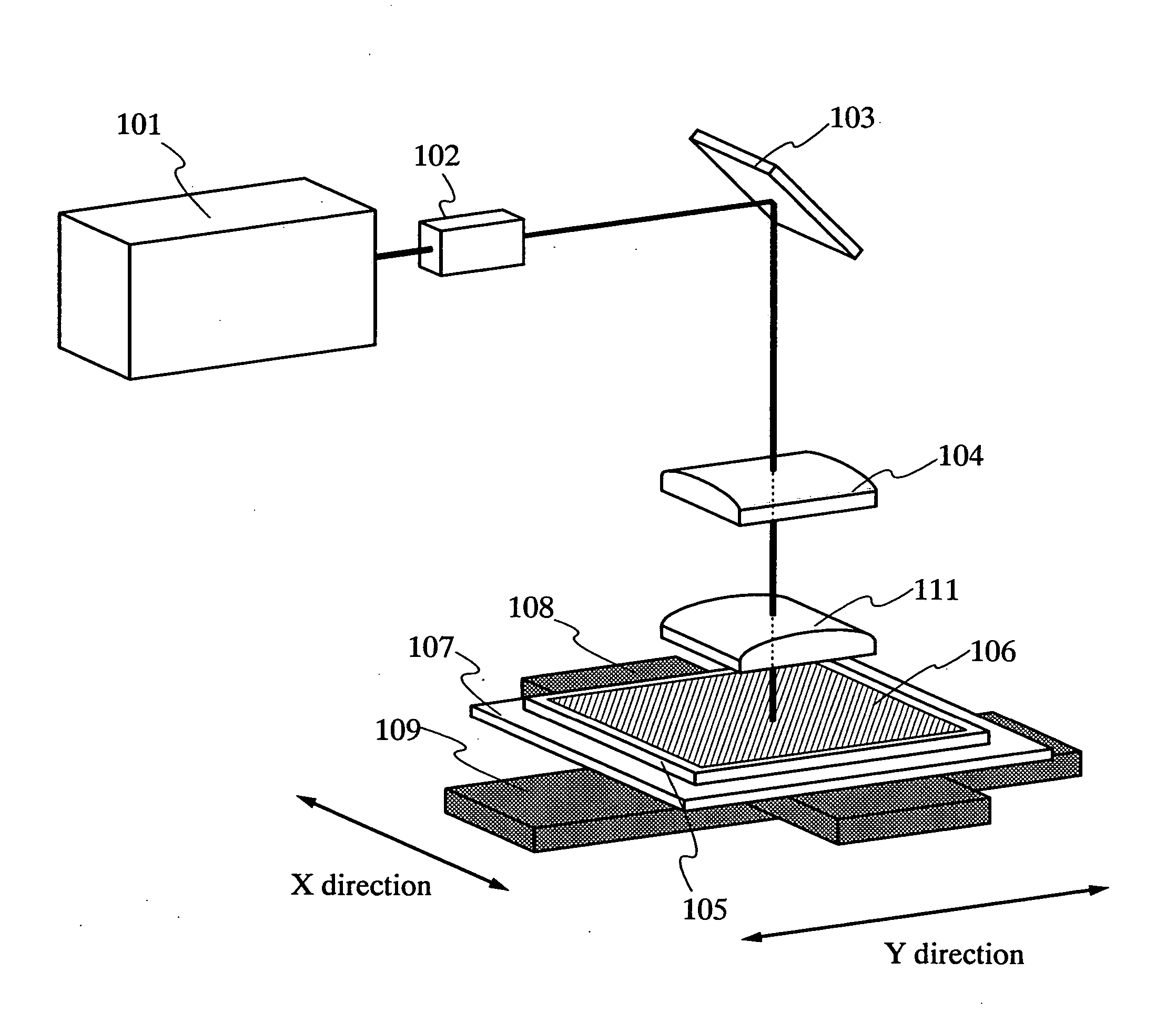
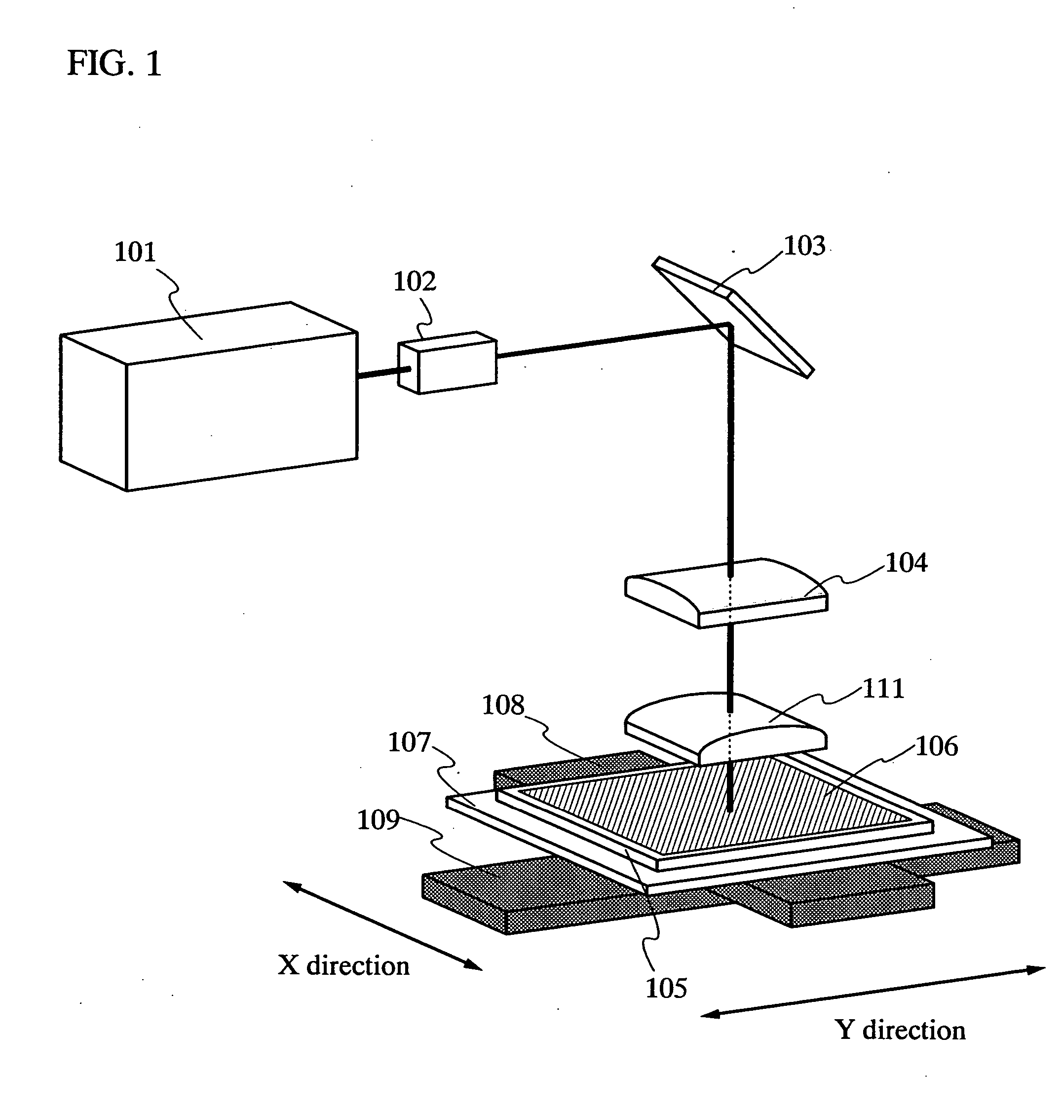
[0058] In FIG. 1, a reference numeral 101 denotes a pulsed laser oscillator. The present invention can be applied to any laser when it can oscillate a laser beam having an ultrashort pulse width of 10 ps or less. For example, an excimer laser, an Ar laser, a Kr laser, a CO2 laser, a YAG laser, a Y2O3 laser, a YVO4 laser, a YLF laser, a YalO3 laser, a GdVO4 laser, a ceramic laser, a glass laser, a ruby laser, an alexandrite laser, a Ti: sapphire laser, a copper vapor laser, or a gold vapor laser can be used.

[0059] This embodiment uses a YVO4 laser having an output power of 8 W. A reference numeral 102 denotes a non-linear optical element. The laser oscillator 101 has a stable resonator and preferably has a spatial profile of TEM00 mode. In the case of TEM00 mode, the laser beam has Gaussian intensity distribution and is superior in focusing property. Therefore, the beam spot can be easily transformed into a desired shape. The laser beam emitted from the laser oscillator is not suffi...

embodiment 2

[0074] This embodiment explains an optical system that can be used in the laser irradiation apparatus of the present invention with reference to FIG. 3.

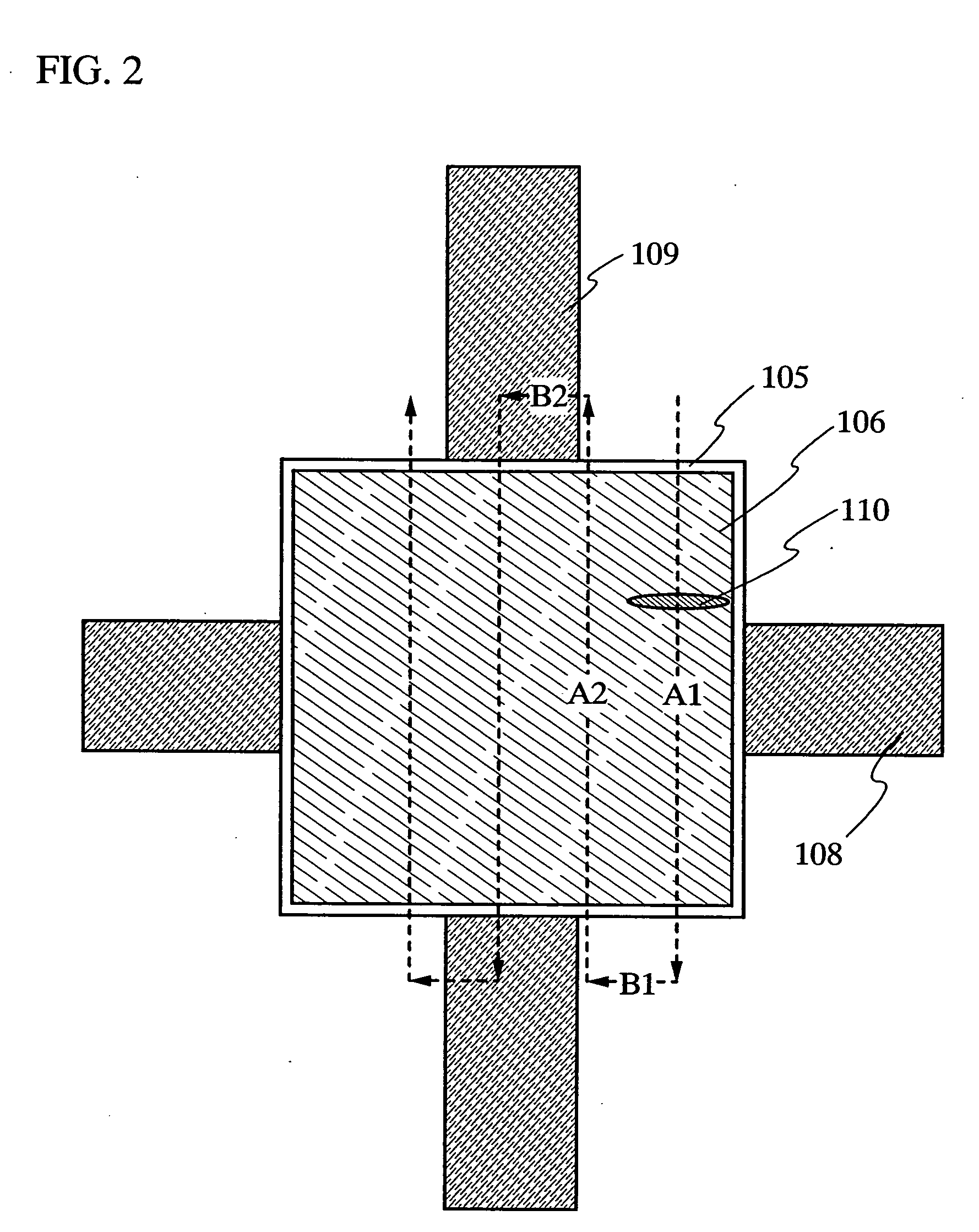
[0075] Since a laser beam is generally emitted to the horizontal direction, the laser beam emitted from the laser oscillator 101 is reflected by a reflecting mirror 103, and its traveling direction is changed so as to have an angle (incident angle) 0 from the vertical direction. In this embodiment mode, the angle θ is 18°. The beam spot of the laser beam whose traveling direction is changed is transformed by a lens 201 and is irradiated to a processing object mounted on a stage 107. In FIG. 3, a semiconductor film 106 formed over a substrate 105 is the processing object. Moreover, in FIG. 3, the reflecting mirror 103 and the lens 104 correspond to the optical system that condenses the laser beam on the semiconductor film 106.

[0076]FIG. 3 shows an example in which a planoconvex spherical lens is used as the lens 201. The planoconvex...

embodiment 3

[0081] When a semiconductor film is irradiated with a continuous wave (CW) laser beam, a crystal grain grown continuously in the scanning direction of the beam spot can be obtained. A region where the crystal grain is grown continuously in the scanning direction has superior crystallinity. Therefore, when this region is used as a channel-forming region of a TFT, a TFT having extremely high mobility and on current can be expected. However, the CW laser has many problems such as a short lifetime of the non-linear optical element, a small beam spot, a serious thermal effect to the substrate, and so on.

[0082] Since the present invention uses the laser beam having an ultrashort pulse width, the pulse repetition rate is high. Therefore, the pulsed laser beam can be emitted after the semiconductor film is melted by the previous laser beam and before the semiconductor film is solidified. This can form a crystal grain grown continuously to the scanning direction of the beam spot, which is t...


PUM

PropertyMeasurementUnit
thicknessaaaaaaaaaa
thicknessaaaaaaaaaa
thicknessaaaaaaaaaa

Abstract

Even when the laser irradiation is performed under the same condition with the energy distribution of the beam spot shaped as appropriate, the energy given to the irradiated surface is not yet homogeneous. When a semiconductor film is crystallized to form a crystalline semiconductor film using such inhomogeneous irradiation energy, the crystallinity becomes inhomogeneous in this film, and the characteristic of semiconductor elements manufactured using this film varies. In the present invention, an irradiated object formed over a substrate is irradiated with a laser beam having the pulse width that is an order of picosecond (10−12 second) or less.

Description

BACKGROUND OF THE INVENTION [0001] 1. Field of the Invention [0002] The present invention relates to a laser irradiation method and particularly relates to a laser irradiation method being able to perform homogeneous annealing to an irradiated object. Moreover, the present invention relates to a method for manufacturing a crystalline semiconductor film and particularly relates to a method for manufacturing a crystalline semiconductor film having less variation of the crystallinity with high throughput. [0003] 2. Related Art [0004] It is important to select a beam profile of a linear beam properly in order to give laser energy homogeneously to the irradiated object in a laser annealing process. [0005] Since a beam spot of a laser beam emitted from a laser oscillator originally has wide energy distribution, the laser irradiation intensity is inhomogeneous according to the location in the irradiated object when the irradiated object is irradiated with the beam spot directly from the la...

Claims


Application Information

Patent Timeline
Patent Type & Authority Applications(United States)
IPC IPC(8): H01L21/324C30B1/00C30B13/06C30B13/24G11B7/00H01L21/20H01L21/268H01L21/336H01L21/77H01L21/84
CPCB23K26/063B23K26/0732B23K26/0736C30B1/00H01L27/1285C30B29/06H01L21/2026H01L29/66757C30B13/24B23K26/0622H01L21/02686H01L21/02678H01L21/02502H01L21/02422H01L21/02488H01L21/02532H01L21/02595H01L21/02691H01L21/324H01L21/268
Inventor TANAKA, KOICHIROYAMAMOTO, YOSHIAKI
Owner SEMICON ENERGY LAB CO LTD
Why Eureka
Try Eureka