Method of manufacturing gallium nitride based semiconductor light emitting device

a technology of gallium nitride and light-emitting devices, which is applied in the direction of basic electric elements, crystal growth processes, chemical instruments and processes, etc., can solve the problems of increasing the operating voltage of the device and the amount of heat, and few methods can be restrictively adopted in practice, so as to prevent deterioration of brightness, reduce the contact resistance, and reduce the operation voltage

Inactive Publication Date: 2005-06-30
SAMSUNG ELECTRONICS CO LTD
View PDF4 Cites 21 Cited by
  • Summary
  • Abstract
  • Description
  • Claims
  • Application Information

AI Technical Summary

Benefits of technology

[0012] The present invention has been made to solve the above problems, and it is an object of the present invention to provide a new method of manufacturing a light emitting diode, which prevents a deterioration in brightness while lowering a contact resistance by removing residual metallic materials after a deposition process of selected metallic materials and heat treatment, in order to lower the contact resistance at a p-type gallium nitride-based semiconductor layer formed with a p-type electrode.

Problems solved by technology

As the GaN-based semiconductor generally has a large energy band gap, there is a difficulty in achieving an ohmic contact with an electrode thereon.
Specifically, a p-type clad layer to be formed with a p-side electrode has a large contact resistance, causing a problem of raising operating voltage of the device and amount of heat.
Thus, only a few methods could be restrictively adopted in practice as a method for lowering the contact resistance.
However, as the transparent electrode 18 is formed of metals, it could be difficult for the transparent electrode to have a desired translucency.
Even though a NiO layer of a relatively high translucency is formed through the heat treatment, it has a transmittance of merely 60%, so that light emitting efficiency can be deteriorated as the transparent electrode thickens.
Thus, the transparent electrode should be limited to a thickness of 100 μm or less, causing a restriction in improving the current injection efficiency.
Further, even though the transparent electrode of the metals has a proper thickness in consideration of a desired transmittance, it inevitably encounters some reduction in brightness due to a restrictive transmittance in the transparent electrode that is made of the metals having a high photon absorption rate, such as Au.

Method used


Image

  • Method of manufacturing gallium nitride based semiconductor light emitting device
  • Method of manufacturing gallium nitride based semiconductor light emitting device
  • Method of manufacturing gallium nitride based semiconductor light emitting device

Examples


Embodiment Construction

[0026] Preferred embodiments will now be described in detail with reference to the accompanying drawings.

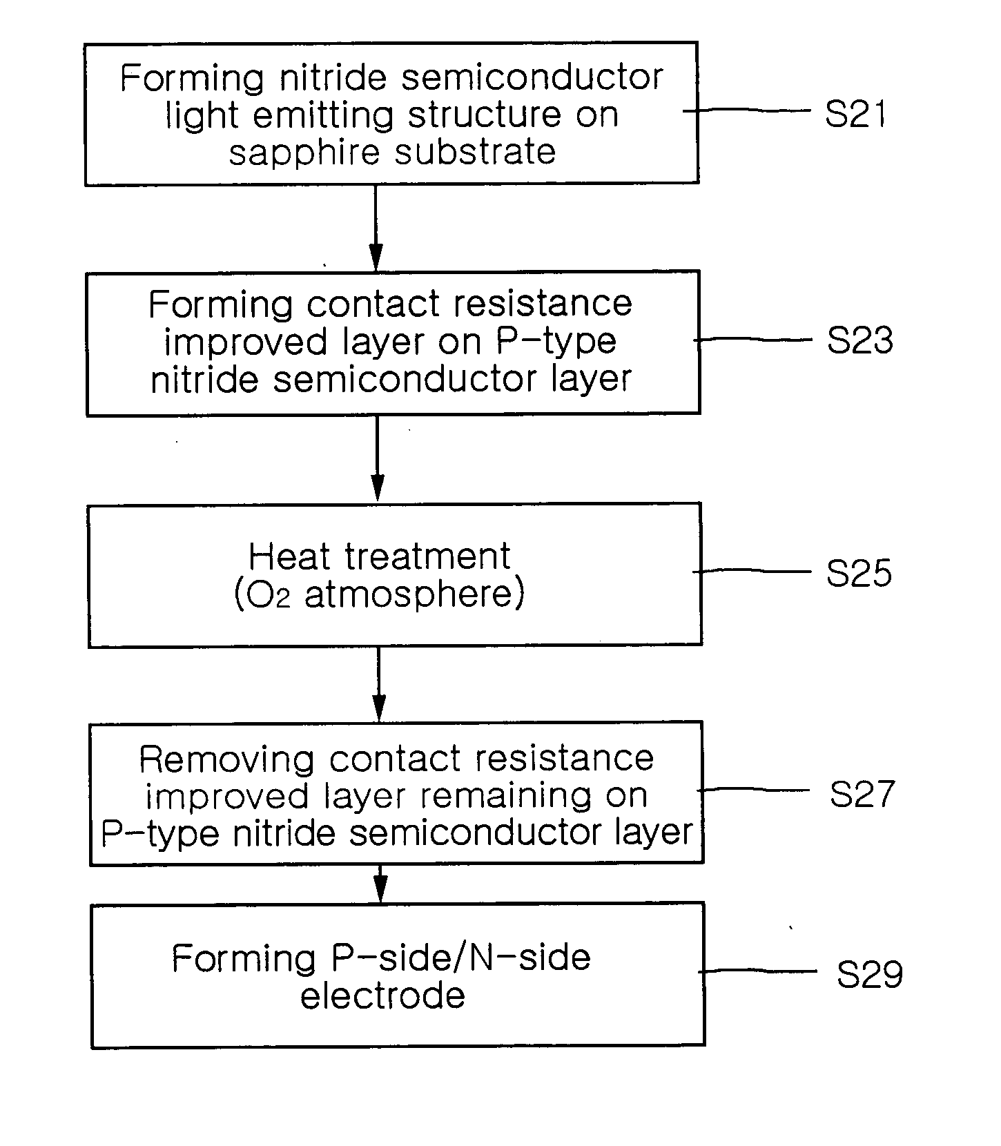
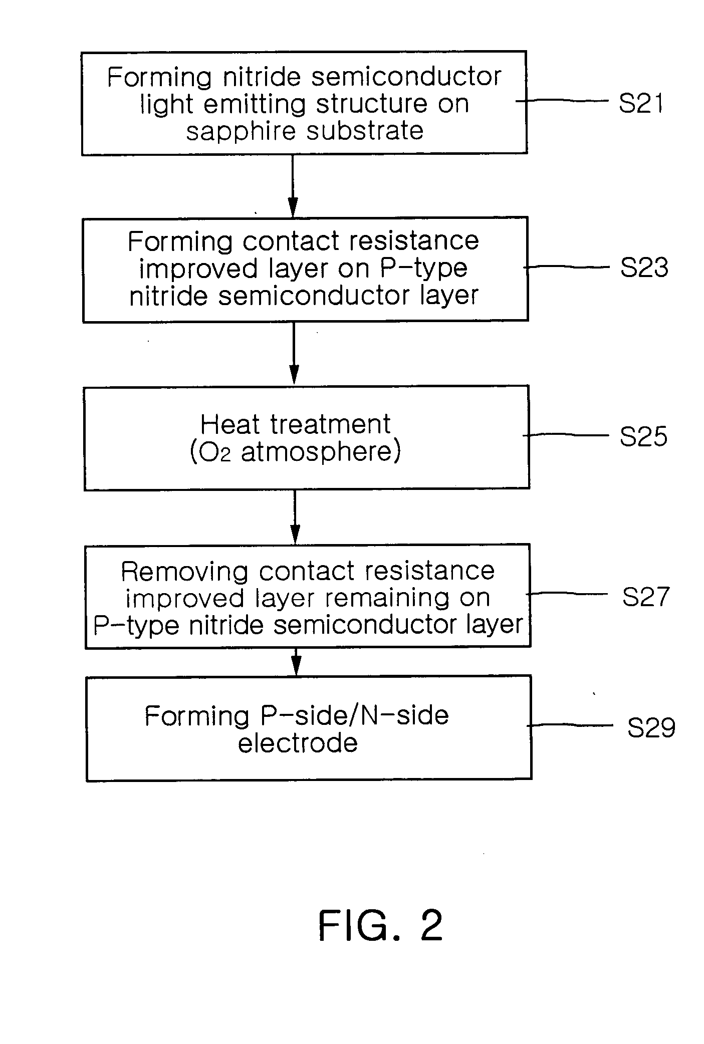
[0027]FIG. 2 is a flow chart illustrating a method of manufacturing a gallium nitride-based light emitting device according to the present invention.

[0028] As shown in FIG. 2, the method of the present invention starts from step S21, at which an n-type GaN-based semiconductor layer, an active layer and a p-type GaN-based semiconductor layer are sequentially formed on a substrate for growing a gallium nitride (GaN)-based semiconductor. As for a substrate for growing a gallium nitride-based semiconductor, a similar GaN substrate, a SiC substrate or a sapphire substrate can be employed, among which the sapphire substrate is generally used.

[0029] Subsequently, at step S23, a contact resistance improved layer is deposited on the p-type GaN-based semiconductor layer. The contact resistance improved layer is a layer for lowering a contact resistance at the surface of the p-type GaN-b...


PUM

PropertyMeasurementUnit
temperatureaaaaaaaaaa
energy band gapaaaaaaaaaa
transmittanceaaaaaaaaaa

Abstract

A method of manufacturing a gallium nitride (GaN)-based semiconductor light emitting device includes forming a contact resistance improved layer on a p-type GaN-based semiconductor layer with at least one metal selected from the group of Au, Mg, Mn, Mo, Pd, Pt, Sn, Ti and Zn, heat-treating the p-type GaN-based semiconductor layer so that elements in the contact resistance improved layer diffuse into the p-type GaN-based semiconductor layer and that Ga elements in the p-type GaN-based semiconductor layer dissolve into the contact resistance improved layer, and removing the contact resistance improved layer remaining on the p-type GaN-based semiconductor layer.

Description

BACKGROUND OF THE INVENTION [0001] 1. Field of the Invention [0002] The present invention relates to a semiconductor light emitting device, and more particularly to a method of manufacturing a gallium nitride (GaN) based semiconductor light emitting device, which ensures a high brightness while lowering a contact resistance near a surface formed with a p-side electrode. [0003] 2. Description of the Related Art [0004] In general, a gallium nitride-based semiconductor is used for a light emitting diode for emitting light in a wavelength range of a blue light or a green light and usually comprises semiconductor materials with the formula AlxInyGa(1-x-y)N (where 0≦x≦1, 0≦y≦1, 0≦x+y≦1). As for the light emitting device generating a green light, a gallium nitride (GaN) semiconductor material with a large energy band gap of about 3.4 eV is usually used. [0005] As the GaN-based semiconductor generally has a large energy band gap, there is a difficulty in achieving an ohmic contact with an e...

Claims


Application Information

Patent Timeline
Patent Type & Authority Applications(United States)
IPC IPC(8): C30B1/00H01L21/00H01L21/20H01L21/306H01L21/36H01L21/425H01L23/48H01L23/52H01L21/28H01L29/40H01L33/06H01L33/10H01L33/32H01L33/40H01L33/62
CPCH01L33/0095H01L33/40H01L33/32H01L33/14
Inventor KIM, HYUN KYUNG
Owner SAMSUNG ELECTRONICS CO LTD
Why Eureka
Try Eureka