Liquid drop jetting apparatus using charged beam and method for manufacturing a pattern using the apparatus

a technology of liquid drop and charging beam, which is applied in the direction of electrostatic spraying apparatus, spraying power supply, coating, etc., can solve the problems of large error in the position where the liquid drop adheres, waste of material, and increased problems, and achieves easy forming, good surface chemical reaction, and increased shaping effect.

Inactive Publication Date: 2005-06-30
SEMICON ENERGY LAB CO LTD
View PDF9 Cites 16 Cited by
  • Summary
  • Abstract
  • Description
  • Claims
  • Application Information

AI Technical Summary

Benefits of technology

[0022] Since the electric charges irradiated needs to be held locally on the surface of the substrate, basically, it is desirable that the surface is covered with an insulating film. In this case, the whole surface is not necessarily covered with the insulating film but it is sufficient for a region required to be patterned to be covered with the insulating film. On the other hand, in the case of forming a pattern also on a surface having a conductive layer partially exposed, the invention does not have an effect on the portion. This is because the conductive body is not charged with the charged beam and hence can not produce an effect of aligning the liquid drops forcibly. In this case, it is required only that the conductive layer is arranged efficiently in the general layout. Hence, it is clear that this does not reduce the effect of the invention itself.
[0023] Another means provided by the invention is to change the physical and / or chemical state of the surface with the charged beam. With this, the adhesion position of the liquid drop discharged from the nozzle can be aligned. This will be described below in a more concrete manner by the use of FIG. 11. A surface is made lyophobic in advance and then a portion irradiated with the charged beam is made lyophilic. The liquid drop remains stably at the lyophilic portion. As a result, the liquid drops are arranged at the portions irradiated with the charged beam. Conversely, it is also recommendable to make the initial state lyophilic and to make the portions irradiated with the beam lyophobic. This change in the state of the surface is effected by promoting the chemical reaction of the surface by the energy of the beam. In addition to this, the state of the surface can be changed by depositing beam constituent atoms in an extremely thin manner on the surface by the use of an ion beam.
[0024] Further, in the invention, it is also effective that the liquid drops are discharged to the substrate from the head to form a pattern and that the pattern is then pressed, for example, by rollers to shape up the pattern. In this case, when the liquid drops are processed before they are subjected to heat treatment, which will be described below, they can be easily shaped and hence a shaping effect can be usually increased. However, depending on the material, it is also recommendable to subject them to the heat treatment and then to press them.
[0025] The main object of the heat treatment described above is to remove quickly unnecessary solvent and the like in the composition that is discharged from the head and adheres to the substrate and to ensure desired material characteristics. For example, in the case of a nano metal particle composition in which ultra-fine metal particles (nano particles) are suspended in a solvent by a surface active substance, in order to reduce the resistance of a metal thin film to be produced to a sufficient extent, it is indispensable to remove the solvent or the surface active substance sufficiently. This requires a temperature higher than a certain degree, for example, annealing at 200° C. or more. Further, in order to enhance the adhesion of the metal particles in the film and to produce a metal film of higher quality, a higher temperature is required.
[0026] The heat treatment holds true not only for the nano metal particles but also, for example, an organic resist material. To perform the heat treatment, it is recommendable to use a lamp annealing unit for heating a substrate directly at a high heating rate by using a lamp such as halogen lamp as a heating source or a laser irradiation unit for irradiating laser light. Both units can subject only a desired portion to the heat treatment by scanning the heating source. As to the other methods, it is also recommendable to use a furnace annealing furnace set at a predetermined temperature, an oven held at 100° C. to 300° C., and the like.
[0027] As described above, the invention for forming the conductive layer by the liquid drop discharge method can manufacture the conductive layer continuously, for example, without exposing the pixel electrode, light emitting layer, and opposite electrode of a light emitting device to the atmosphere if the composition discharged from the head is changed or the head filled with the composition is changed.

Problems solved by technology

Still further, since the conductive layer is once formed over the whole area and then is etched in such a way as to form a desired shape, wasted material is generated.
These problems become more serious in the case of forming a wiring on a large size substrate having a side exceeding at least 1 m.
However, in the case of discharging these liquid drops by the liquid drop discharge method, a small fluctuation in a direction of discharge of the liquid drop causes a large error in the position where the liquid drop adheres.
For this reason, even if the amount of discharge of the liquid drop itself is reduced, a limit is brought to the accuracy of the pattern.
Moreover, if the amount of liquid drops is reduced excessively, there is presented not only a problem of reducing throughput but also a problem of reducing also the very accuracy of adhesion of the liquid drop reversely.

Method used


Image

  • Liquid drop jetting apparatus using charged beam and method for manufacturing a pattern using the apparatus
  • Liquid drop jetting apparatus using charged beam and method for manufacturing a pattern using the apparatus
  • Liquid drop jetting apparatus using charged beam and method for manufacturing a pattern using the apparatus

Examples


embodiments

Embodiment 1

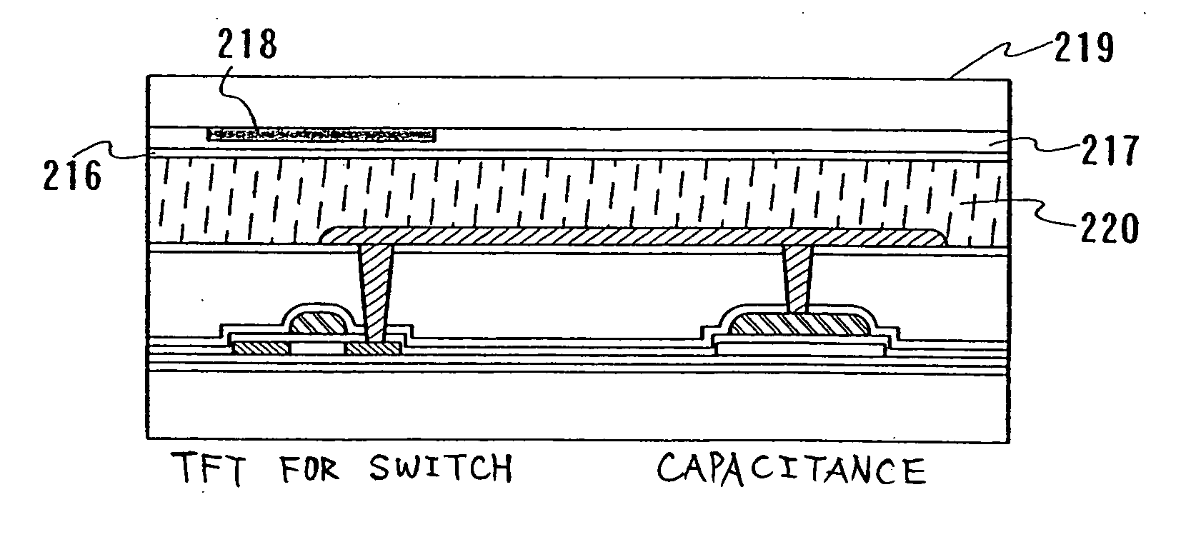
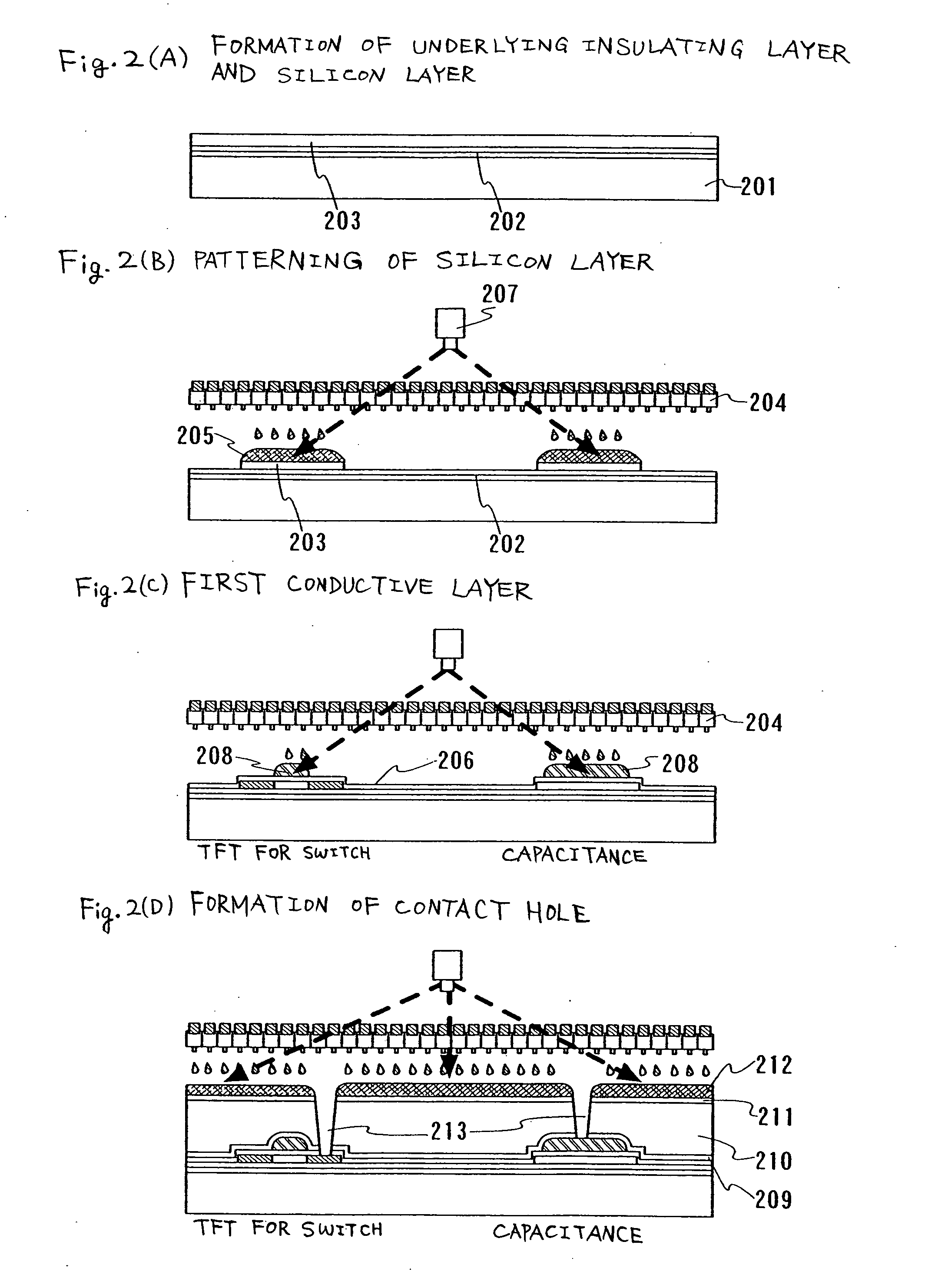
[0062] The first embodiment of the invention will be described in detail by the use of FIGS. 2 and 3. In the invention, an active matrix type liquid crystal display device is made by a patterning process using a liquid drop discharge method without using a patterning process using a conventional photolithography. In the construction of the invention to be described below, reference symbols designating the same parts are used in common throughout the different drawings. Here, a process for manufacturing an N channel type TFT (for switch) and a capacitance on the same substrate will be described.

[0063] A substrate resistant to the processing temperature of this process such as a glass substrate and a flexible substrate typified by a plastic substrate is used as the substrate 201 (FIG. 2(A)). To be specific, an active matrix substrate is manufactured by the use of the substrate 201 having transparence. As to a substrate size, it is preferable that a large area substrate s...

embodiment 2

[0090] The second embodiment of the invention will be described in detail by the use of FIGS. 4 and 5. Also in this embodiment, an EL display device is manufactured by a patterning process of using electron beam irradiation and liquid drop discharge in combination without using a patterning process of using a conventional lithography method. Incidentally, in the construction of the invention to be described below, the reference symbols designating the same parts are used in common throughout the different drawings. Here, a process of manufacturing an EL display device will be described by which an N channel type TFT (for switch) and two P channel type TFTs (for driving) are formed on the same substrate by the use of the invention. In this regard, the detailed descriptions of the same parts as those in the first embodiment will be omitted.

[0091] A substrate resistant to a treatment temperature in this process, for example, a glass substrate and a flexible substrate typified by a pla...

embodiment 3

[0109] In this embodiment, a method of filling a contact hole (open hole) with a liquid drop composition by using the liquid drop discharge method will be described by the use of FIGS. 7 to 9.

[0110] In FIG. 7(A), a semiconductor 3001 is formed over a substrate 3000 and an insulator 3002 is formed over the semiconductor 3001 and the insulator 3002 has a contact hole 3003. A publicly known method can be used as a method of forming a contact hole but a liquid drop discharge method may be also used. In this case, a wet etching solution is discharged from a nozzle to form the contact hole 3003. Then, the contact hole and the wiring can be continuously formed by the liquid drop discharge method.

[0111] Then, a nozzle 3004 is moved above the contact hole 3003 and a liquid drop composition is continuously discharged to the contact hole 3003 to fill the contact hole 3003 with the liquid drop composition (FIG. 7(B)). Then, by resetting the position of the nozzle 3004 and discharging the liqu...


PUM


Abstract

The invention drastically improves the accuracy of adhesion position of a liquid drop discharged by a liquid drop discharge method and makes it possible to form a fine and highly accurate pattern directly on a substrate. Therefore, one object of the invention is to provide a method for manufacturing a wiring, a conductive layer and a display device that can respond to upsizing of a substrate. Moreover, another object of the invention is to provide a method for manufacturing a wiring, a conductive layer and a display device that can improve throughput and the efficiency of use of material. The invention can improve the accuracy of adhesion position of a liquid drop drastically at the time of patterning a resist material, a wiring material, or the like directly by the liquid drop discharge method mainly on a substrate having an insulating surface. To be more specific, the invention is characterized in that: a liquid adhesion position on the surface of the substrate is scanned with a charged beam in accordance with a desired pattern immediately before a liquid drop is discharged by the liquid drop discharge method; and immediately thereafter, the liquid drop is charged with an electric charge of a polarity opposite to the charged beam and is discharged to improve the controllability of the adhesion position of the liquid drop to a great extent.

Description

TECHNICAL FIELD [0001] The present invention relates to a liquid drop discharge apparatus for producing a fine pattern directly on a substrate and a method for forming a wiring or forming a pattern of a resist or the like by the use of the apparatus. BACKGROUND ART [0002] A thin film transistor (TFT) formed by the use of a thin film on an insulating surface is widely applied to an integrated circuit and the like and is used as a switching device in many cases. A display panel using the TFT has been widely used especially for a large size display device and hence there has been a growing demand for the higher definition, higher aperture ratio, higher reliability, and upsizing of a screen size. [0003] Among methods for making a wiring in a thin film transistor like this is a method for forming a film of a conductive layer on the whole area of a substrate and then etching the film by using a mask (see patent document 1). [Patent Document 1] JP-A-2002-359246 Disclosure of the Inventio...

Claims


Application Information

Patent Timeline
Patent Type & Authority Applications(United States)
IPC IPC(8): B05B5/025B05B5/053B05B12/12B05C5/00B05C5/02H01L21/26H01L21/324H01L21/42H01L21/477
CPCB05B5/025B05B5/053B05C5/0279B05C5/0212B05B12/12B41J2/08
Inventor IMAI, KEITAROYAMAZAKI, SHUNPEI
Owner SEMICON ENERGY LAB CO LTD
Why Eureka
Try Eureka