Nonvolatile semiconductor memory device

a semiconductor and memory device technology, applied in semiconductor devices, digital storage, instruments, etc., can solve the problems of high consumption power, difficulty in miniaturization, miniaturization and high speed operation

Active Publication Date: 2005-07-14
XENOGENIC DEV LLC
View PDF8 Cites 43 Cited by
  • Summary
  • Abstract
  • Description
  • Claims
  • Application Information

AI Technical Summary

Benefits of technology

[0018] According to a third aspect of the present invention, more preferably, in the nonvolatile semiconductor memory device according to any of the above aspects, the variable resistor is a praseodymium-calcium-manganese oxide represented by a general formula, Pr1-xCaxMnO3, which has been formed at a film forming temperature from 350° C. to 500° C. A Pr1-xCaxMnO3 (PCMO) film formed at a film forming temperature from 350° C. to 500° C. is in a state where crystallinity and amorphism are mixed. Therefore, the nonvolatile semiconductor memory device can exhibit the working effects resulting from the first aspect while having properties of great resistance variation of the PCMO film.
[0019] According to a fourth aspect of the present invention, more preferably, in the nonvolatile semiconductor memory device according to any of the above aspects, the variable resistor is formed in a layer above the lowest metal interconnect layer. In the case where a memory cell is assumed to be formed of a variable resistance element and an active element such as a transistor, the variable resistance element and the transistor can be placed on top of each other; therefore, reduction in the size of the memory cell can be achieved. In addition, since the variable resistor can be formed in a process at a low temperature, thermal damage to the metal interconnect that has been placed in a lower layer can be avoided.
[0021] In the nonvolatile semiconductor memory device according to the fifth aspect, since the initial resistance value of the variable resistor varies depending on the annealing process after the film-formation, it is possible to set an initial resistance value in the subsequent annealing process in a temperature range that allows the state where crystallinity and amorphism are mixed to be maintained, so as to make the variable resistance element appropriately operable in accordance with the required properties without changing the geometrical dimensions of the variable resistor, such as the film thickness, wherein a variable resistor having a resistance which is too low is avoided, even in the case where the variable resistor is in an amorphous state or in a state where crystallinity and amorphism are mixed, and has a resistance higher than the appropriate initial resistance value at the time of the film-formation.

Problems solved by technology

However, these memory devices at the present stage have their merits and demerits, and there is a long way to go before the realization of an ideal “universal memory” which has the respective merits of an SRAM, a DRAM and a flash memory.
The FeRAM, for example, which has already been put into practice, utilizes a spontaneous polarization inversion phenomenon of oxide ferroelectrics and is characterized by a low consumed power and a high speed operation; however, it is inferior due to high cost and destructive readout.
This element has a large problem of high consumed power for magnetization inversion at the time of programming and of a difficulty in miniaturization.
In addition, the OUM based on thermal phase transformation of a chalcogenide material is advantageous in low cost and process matching; however, it has a problem in miniaturization and in a high speed operation due to its thermal operation.

Method used


Image

  • Nonvolatile semiconductor memory device
  • Nonvolatile semiconductor memory device
  • Nonvolatile semiconductor memory device

Examples


Embodiment Construction

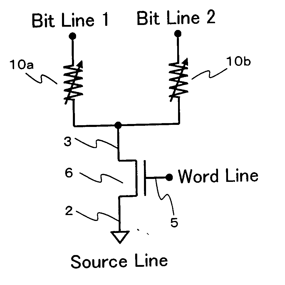
[0033] One embodiment of a nonvolatile semiconductor memory device according to the present invention (hereinafter, appropriately referred to as “inventive device”) is described below with reference to the drawings.

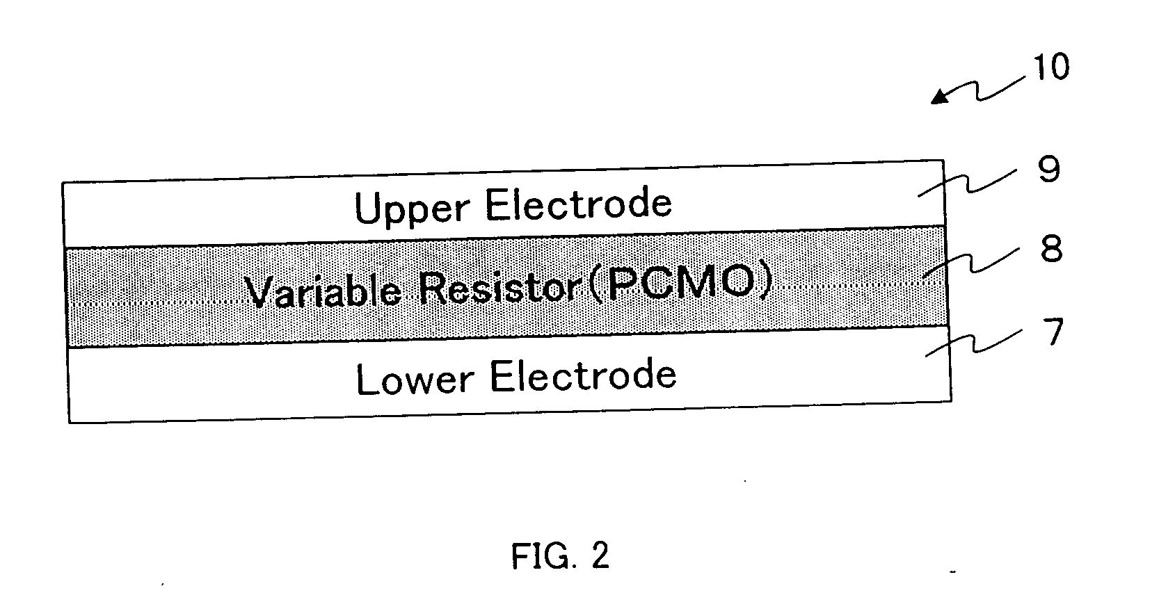
[0034]FIG. 2 is a cross sectional diagram showing the basic structure of a variable resistive element 10 which is a nonvolatile memory element used in an inventive device 100. The basic element structure of variable resistive element 10 is a layered structure where a lower electrode 7, a variable resistor 8 made of a perovskite-type metal oxide film, and an upper electrode 9 are layered in sequence.

[0035] As for the perovskite-type metal oxide that is used as the variable resistor 8, a great number of examples such as Pr1-xCaxMnO3 (PCMO), Pr1-x(Ca,Sr)xMnO3, Nd0.5Sr0.5MnO3, La1-xCaxMnO3, La1-xSrxMnO3 and Gd0.7Ca0.3BaCo2O5+5 are known. Among these, Pr1-xCaxMnO3-based materials, which have a large distortion in the network of the transition metal-oxide bonding and where a ...


PUM


Abstract

A nonvolatile memory element is formed by layering a lower electrode, a variable resistor and an upper electrode in sequence. The variable resistor is formed in which crystallinity and amorphism are mixed. Thus, the nonvolatile memory element is formed. More preferably, the variable resistor is a praseodymium-calcium-manganese oxide represented by a general formula, Pr1-xCaxMnO3, that has been formed at a film forming temperature from 350° C. to 500° C. Alternatively, the variable resistor is formed as a film at a film forming temperature that allows the variable resistor to become of an amorphous state or a state where crystallinity and amorphism are mixed and, then, is subjected to an annealing process at a temperature higher than the film forming temperature, in a temperature range where the variable resistor can maintain the state where crystallinity and amorphism are mixed.

Description

CROSS REFERENCE TO RELATED APPLICATIONS [0001] This Nonprovisional application claims priority under 35 U.S.C. §119(a) on Patent Application No. 2004-006321 filed in Japan on Jan. 14, 2004, the entire contents of which are hereby incorporated by reference. BACKGROUND OF THE INVENTION [0002] 1. Field of the Invention [0003] The present invention relates to a nonvolatile semiconductor memory device and, more specifically, to a manufacturing method of a nonvolatile semiconductor memory device including a variable resistive element having a variable resistor made of a perovskite-type metal oxide film. [0004] 2. Description of the Related Art [0005] In recent years, a variety of device structures such as an FeRAM (Ferroelectric RAM), an MRAM (Magnetic RAM) and an OUM (Ovonic Unified Memory) have been proposed as a next generation nonvolatile random access memory (NVRAM) that makes a rapid operation possible substituting a flash memory, and there has been a fierce competition for the deve...

Claims


Application Information

Patent Timeline
Patent Type & Authority Applications(United States)
IPC IPC(8): H01L27/105G11C13/00G11C16/02H01L27/115H01L27/24H01L45/00
CPCG11C13/0007G11C13/003G11C2213/31G11C2213/78G11C2213/79H01L45/1641H01L45/04H01L45/1233H01L45/147H01L45/1625H01L27/2436H10B63/30H10N70/20H10N70/8836H10N70/041H10N70/026H10N70/826
Inventor KAWAZOE, HIDECHIKATAMAI, YUKIOSHIMAOKA, ATSUSHIHAGIWARA, NAOTOMASUDA, HIDETOSHISUZUKI, TOSHIMASA
Owner XENOGENIC DEV LLC
Why Eureka
Try Eureka