Method for forming pattern of stacked film and thin film transistor

a technology of stacked film and thin film, which is applied in the direction of basic electric elements, electrical appliances, semiconductor devices, etc., can solve the problems of difficult control of the dimension of the polysilicon film and the switch off of the tft, the three-layer film does not cover the sidewall step portion of the two-layer structure, and the etching of the lower oxide film

Active Publication Date: 2005-07-21
HANNSTAR DISPLAY CORPORATION
View PDF12 Cites 27 Cited by
  • Summary
  • Abstract
  • Description
  • Claims
  • Application Information

AI Technical Summary

Benefits of technology

[0029] Therefore, an object of the present invention is to provide a method of forming a pattern of a stacked film and a thin film transistor which suppress the influence that the electric potential of a light shielding film affects to an operation of the thin film transistor, in the thin film transistor having a structure which has the light shielding film under an island of a semiconductor.
[0030] Another object of the present invention is to provide a method of forming a pattern of a stacked film and a thin film transistor which reduce operation malfunctions and display defects, and improves production yield and reliability to reduce a cost.
[0031] Still another object of the present invention to provide, with regard to a stacked structure of a lower oxide film, a semiconductor film and an upper oxide film, a method for forming a pattern of a stacked film composed of a semiconductor film and an upper oxide film, the pattern of the stacked film being capable of absorbing a physical stress on an insulating film and wiring, which cover the pattern of the stacked film, and capable of preventing a crack of the insulating film and a disconnection.

Problems solved by technology

If the film thickness of the upper oxide film is thickened more than 10 nm, then the time necessary for the diluted hydrofluoric acid treatment, required for removing the overhang, must be more than 10 seconds, and an excessive etching of the lower oxide film occurs on an interface between the polysilicon film and the lower oxide film.
In addition, if the polysilicon film is thickened to more than 60 nm, then variations in etching in the case of selectively removing the polysilicon film by etching are increased, thus making it difficult to control the dimension of the polysilicon film and to switch off the TFT.
This means that the three-layer film does not sufficiently cover the sidewall step portion of the two-layer structure.
In general, the surface of the polysilicon film configuring the two-layer structure is uneven, and its morphology is bad.
Therefore, it is thought that the gate oxide film and the gate electrode on the two-layer structure are not evenly deposited and that the cracks become prone to occur on the thin portions of the gate oxide film and gate electrode.
In the active matrix-type liquid crystal display, one of the problems related to light is leak current (light leak current) caused by the generation of electric carriers of the light excitation in response to light reaching to the thin film transistors.
However, the written voltage has declined when the light leak current is large and brings about the decline of the contrast.

Method used


Image

  • Method for forming pattern of stacked film and thin film transistor
  • Method for forming pattern of stacked film and thin film transistor
  • Method for forming pattern of stacked film and thin film transistor

Examples


first embodiment

[0061] A first embodiment of a method for forming a pattern of a stacked film and a thin film transistor according to the present invention will be described below with reference to the attached drawings.

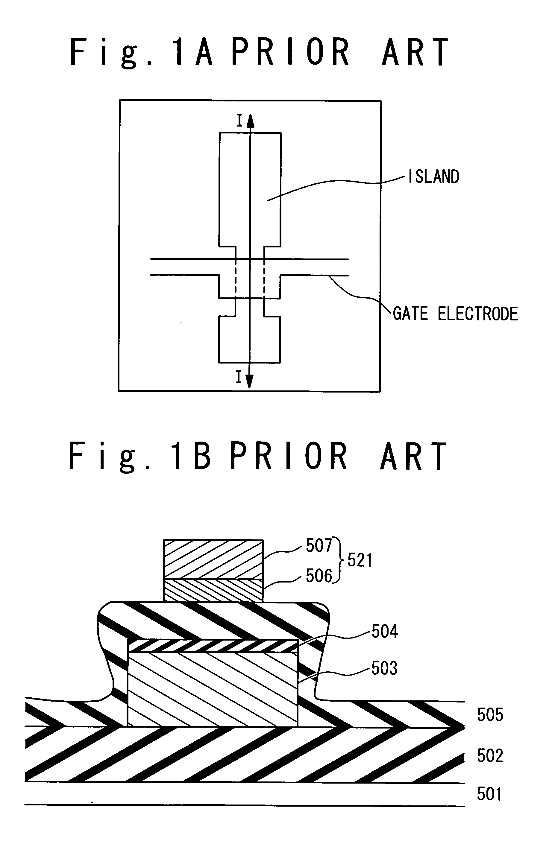
[0062]FIG. 4 is a cross-sectional view showing a configuration of a thin film transistor of the embodiments. The thin film transistor is provided on a glass substrate 101. The thin film transistor includes a lower oxide film 102, a polysilicon film 103, an upper oxide film 104, a gate oxide film 105, a micro-crystalline silicon (μc-Si) film 106, Cr film 107, a first interlayer oxide film 109, a second interlayer oxide film 112, contacts 113 and aluminum wirings 114.

[0063] The lower oxide film 102 is formed in a thickness of approximately 300 nm on the glass substrate 101. The polysilicon film 103 and the upper oxide film 104, which configure a two-layer structure, are provided in thicknesses of 60 nm and 10 nm, respectively, on the lower oxide film 102. Here, the polysilicon film ...

second embodiment

[0103] Next, a second embodiment of the method for forming a pattern of a stacked film of the present invention will be described. In the second embodiment, the etching time for the reactive ion etching by the gas containing CF4 and O2 when forming the two-layer structure is shortened.

[0104]FIG. 10 is a graph showing RF power dependencies of etching rates, for respective films, of etching gases for use in the second embodiment. Similarly to the first embodiment, the upper oxide film and the polysilicon film undergo the reactive ion etching by the gas series of CF4 and O2 by use of the photoresist as an etching mask until the lower oxide film is exposed. In this case, in the second embodiment, the etching conditions are set as: [0105] Gas flow amount ratio of CF4 and O2:1:1; [0106] Total gas flow amount: 200 sccm; [0107] Gas pressure: 20 Pa; and [0108] RF power: 300 W and 500 W

When the RF power is increased from 300 W to 500 W, though the etching rate for the polysilicon film is a...

third embodiment

[0111] The third embodiment in the method for forming the pattern of the stacked film and the thin film transistor of the present invention will be described below.

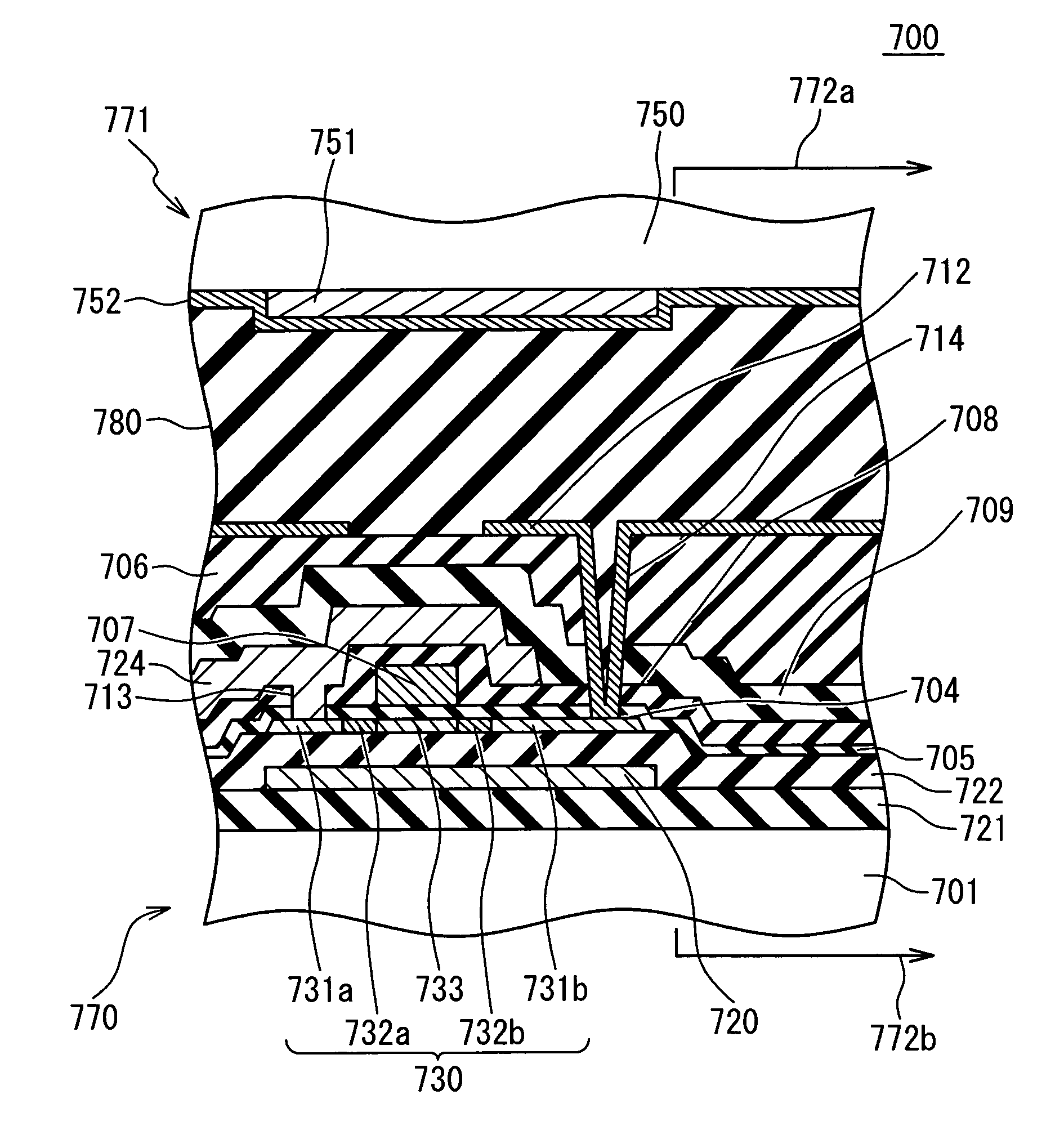
[0112] At first, the configuration of the third embodiment of the method for forming the pattern of the stacked film and the thin film transistor in the present invention is explained. FIG. 11 is a cross-sectional view showing the configuration of a liquid crystal light valve to which the third embodiment of the present invention are applied. The liquid crystal light valve 700 includes a TFT array substrate 770, an opposite substrate 771 and a liquid crystal 780.

[0113] The TFT array substrate 770 has a plurality of thin film transistors arrayed like a matrix and a plurality of pixel electrodes that are turned on and off by the thin film transistors. The opposite substrate 771 has the common opposite electrode opposite to the plurality of pixel electrodes of the TFT array substrate 770. The liquid crystal 780 is put and ...


PUM


Abstract

A method for forming a pattern of a stacked film, includes steps (a) to (e). The step (a) is forming sequentially a first base insulating film and a light shielding material on a transparent substrate. The step (b) is patterning the light shielding material to obtain a light shielding film with a first pattern. The step (c) is forming sequentially a second base insulating film, a semiconductor film and a first oxide film on a substrate. The step (d) is forming a resist pattern with a second pattern on the first oxide film. The step (e) is forming a pattern of a stacked film by dry etching the first oxide film and the semiconductor film, above the light shielding film. The stacked film includes the semiconductor film and the first oxide film. The dry etching includes an etching by using an etching gas and the resist pattern as a mask. The semiconductor film includes a taper angle which is controlled to be within predetermined range.

Description

CROSS REFERENCE TO RELATED APPLICATIONS [0001] This application is a continuation-in-part of U.S. patent application Ser. No. 10 / 446,713 filed on May 29, 2003, which is pending, the contents of which are hereby incorporated by reference. This application relates to U.S. patent application Ser. No. 10 / 855,394 filed on May 28, 2004, which is pending, the contents of which are hereby incorporated by reference. The present application claims the benefit of Japanese patent application No. 2003-161207, filed in Japan on Jun. 5, 2003, the subject matter of which is hereby incorporated herein by reference.BACKGROUND OF THE INVENTION [0002] 1. Field of the Invention[0003] The present invention relates to a method for forming a pattern of a stacked film and a thin film transistor, and more particularly, to a method for forming a pattern of a stacked film composed of a polysilicon film and an upper oxide film and a thin film transistor having the stacked film. [0004] 2. Description of the Rela...

Claims


Application Information

Patent Timeline
Patent Type & Authority Applications(United States)
IPC IPC(8): H01L21/311H01L21/3213H01L21/336
CPCH01L21/31116H01L21/32137H01L29/78636H01L29/78633H01L29/66757
Inventor SEKO, NOBUYASHIRAISHI, HITOSHIHAYASHI, KENICHIHIRANO, NAOTOYAMAMOTO, ATSUSHI
Owner HANNSTAR DISPLAY CORPORATION
Why Eureka
Try Eureka