Optical deflection element and method of producing the same

a technology of optical deflection element and optical deflection element, which is applied in the field of optical deflection element and the field of producing the same, can solve the problems of difficult to obtain single crystal oxide film, difficult to make them large, and difficulty in practical use, and achieve the effects of good crystallinity, and improving the crystallinity of magnesia spinel film

Inactive Publication Date: 2005-07-28
FUJITSU LTD
View PDF6 Cites 8 Cited by
  • Summary
  • Abstract
  • Description
  • Claims
  • Application Information

AI Technical Summary

Benefits of technology

[0030] Between the step of forming the intermediate layer and the step of forming the lower electrode, there may be further a step of a thermal treatment in an atmosphere including oxygen gas or water vapor. Due to the thermal treatment, a thermal oxide film is formed at an interface between the intermediate layer and the single crystal substrate. Hence, bonding is eliminated between the single crystal substrate having a heteroepitaxial structure and the intermediate layer, and this enables self re-arrangement of the magnesia spinel film, which functions as the intermediate layer, by a thermal treatment. As a result, the crystallinity of the magnesia spinel film are further improved, and the lower electrode, the first oxide layer, and the second oxide layer formed on the magnesia spinel film accede the good crystallinity, and the crystallinity of them are also improved.

Problems solved by technology

However, in many cases, it is difficult to obtain single crystal oxide films, and usually only polycrystalline films can be obtained.
However, the commonly used oxide single crystal substrates are about 2 inches in size, and it is difficult to make them large.
In addition, from the point of view of price, there are also difficulties in practical use, because a two-inch MgO substrate costs as much as several hundreds thousands Yen, while a six-inch silicon single crystal substrate costs only a few thousands yen.
Because the silicon oxide film formed by thermal oxidation is amorphous, and does not have a specific orientation, an epitaxial film cannot be grown on this silicon oxide film.
However, if the conductive film is not sufficiently crystallized, the crystalline arrangement of the perovskite oxide film degrades, resulting in an increase in optical propagation loss, and degradation of the electro-optical effect.

Method used


Image

  • Optical deflection element and method of producing the same
  • Optical deflection element and method of producing the same
  • Optical deflection element and method of producing the same

Examples


first embodiment

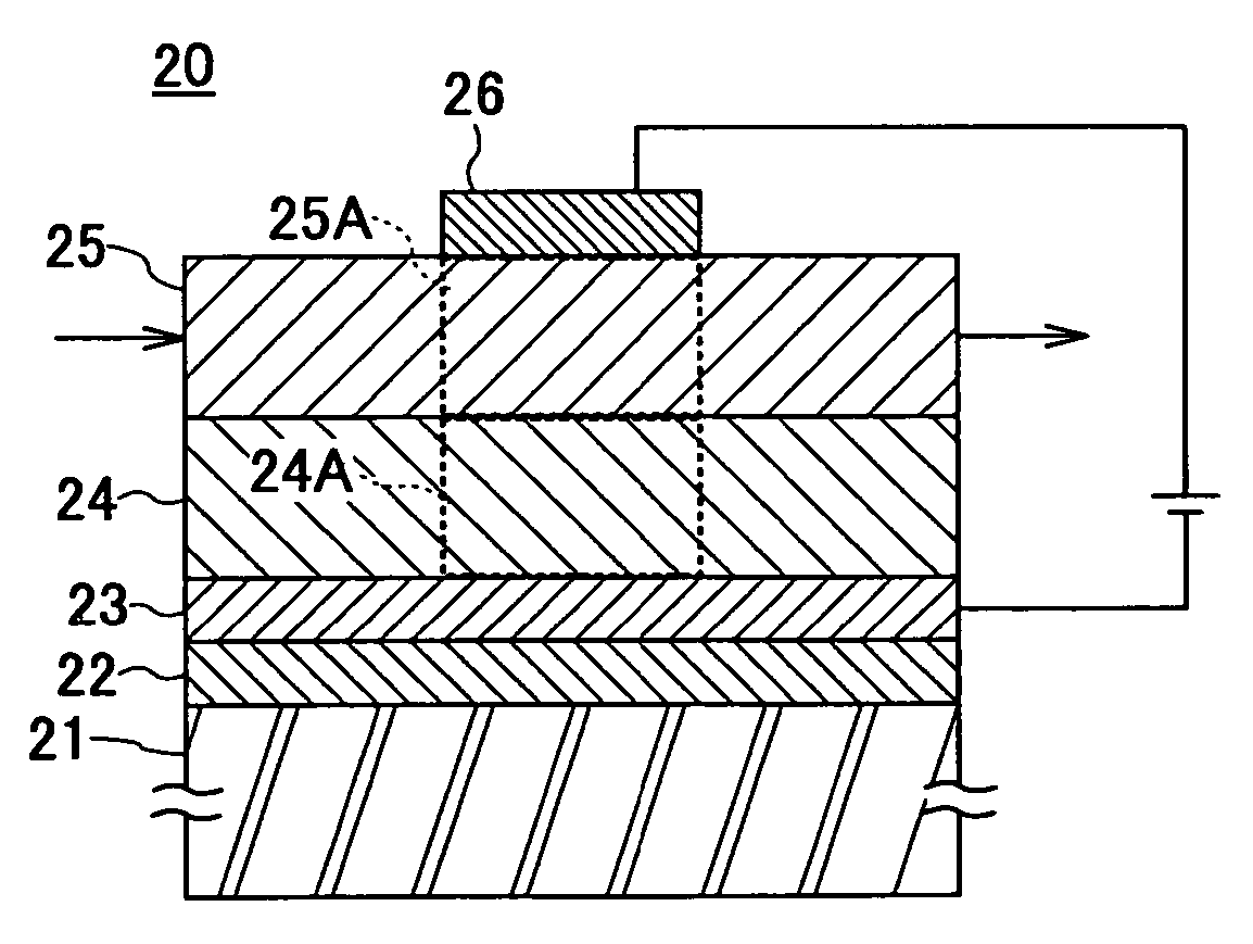
[0098]FIG. 7 is a plan view of an optical deflection element according to a first embodiment of the present invention.

[0099]FIG. 8 is a cross-sectional view of the optical deflection element according to the first embodiment of the present invention.

[0100] As illustrated in FIG. 7 and FIG. 8, the optical deflection element 20 of the present embodiment includes a magnesia spinel film 22, a lower electrode 23, a lower cladding layer 24, a core layer 25, and an upper electrode 26, which are sequentially stacked on a silicon single crystal substrate 21. The magnesia spinel film 22, the lower electrode 23, a PLZT film acting as the lower cladding layer 24, and a PZT film acting as the core layer 25 are epitaxially grown on respective underlying layers thereof and accede the crystallinity of the respective underlying layers.

[0101] The optical deflection element 20 is a waveguide optical deflection element. Here, for example, the refractive index of the PZT core layer 25 is set to be 2....

second embodiment

[0123] The optical deflection element of the present embodiment is basically the same as the optical deflection element 20 of the first embodiment, except that an upper cladding layer is further provided on the core layer.

[0124]FIG. 9 is a cross-sectional view of an optical deflection element according to the second embodiment of the present invention. In FIG. 9, the same reference numbers are assigned to the same elements as previously described, and overlapping descriptions are omitted.

[0125] As illustrated in FIG. 9, an optical deflection element 30 of the present embodiment includes a magnesia spinel film 22, a lower electrode 23, a lower cladding layer 24, a core layer 25, an upper cladding layer 31, and an upper electrode 26, which are sequentially stacked on a silicon single crystal substrate 21. Among the above films, the magnesia spinel film 22, the lower electrode 23, the PLZT lower cladding layer 24, the PZT core layer 25, and the PLZT upper cladding layer 31 are epitax...

third embodiment

[0133] The optical deflection element of the present embodiment is basically the same as the optical deflection element 30 of the second embodiment, except that an iridium film is formed to replace the platinum lower electrode 23. Below, descriptions of the same fabrication process as that in the second embodiment are omitted, and reference numbers in FIG. 9 are used, which illustrates the optical deflection element 30 of the second embodiment.

[0134] The iridium film is formed on the magnesia-spinel layer 22 by sputtering to 200 nm. Specifically, the pressure in a sputtering chamber is set to be 1 Pa (7.5×10⁻³ Torr), and the substrate is heated to 600° C. to epitaxially grow the iridium film while supplying argon gas at 30 sccm and oxygen gas at 1 sccm.

[0135] According to the present embodiment, the growing direction of the iridium film is (001), the in-plane orientation of the iridium film is [001], the same as [001] of the other layers.


PUM

PropertyMeasurementUnit
sizeaaaaaaaaaa
thicknessaaaaaaaaaa
thicknessaaaaaaaaaa

Abstract

A disclosed optical deflection element includes a magnesia spinel film 22, a lower electrode 23, a lower cladding layer 24, a core layer 25, and an upper cladding layer 26, which are sequentially stacked formed on a silicon single crystal substrate 21. The magnesia spinel film 22, the lower electrode 23, a PLZT film acting as the lower cladding layer 24, and a PZT film acting as the core layer 25 are epitaxially grown on respective underlying layers thereof. Because of a voltage applied between the lower electrode 23 and the upper electrode 26, refractive index variable regions 25A, 24A, in which the refractive index varies, are formed due to the electro-optical effect. Light incident into the core layer 25 is deflected at the interface between the core layer 25 and the refractive index variable regions 25A, 24A to the inner side relative to the surface of the core layer 25.

Description

CROSS-REFERENCE TO RELATED APPLICATION [0001] This application is a U.S. continuation application filed under 35 USC 111(a) claiming benefit under 35 USC 120 and 365(c) of PCT application JP03 / 000736, filed Jan. 27, 2003. The application is hereby incorporated herein by reference.TECHNICAL FIELD [0002] The present invention generally relates to an optical deflection element utilized in optical communication and a method of producing the optical deflection element, and particularly, to an optical deflection element that deflects a light beam in an optical waveguide by an electro-optical effect, and a method of producing the optical deflection element. TECHNICAL BACKGROUND [0003] Along with growing capacity of data transmitted in communication, optical communication technology using light as a medium becomes more and more important. Especially, fiber networks have been extended to homes, and it is expected that users will rapidly increase. In order for a large number of users of the f...

Claims


Application Information

Patent Timeline
Patent Type & Authority Applications(United States)
IPC IPC(8): G02F1/055G02F1/1337G02F1/295
CPCG02F1/055G02F1/0553G02F1/295
Inventor KONDO, MASAOYAMAWAKI, HIDEKI
Owner FUJITSU LTD
Why Eureka
Try Eureka