

Synergetic SP-SP2-SP3 carbon materials and deposition methods thereof
a carbon material and synergetic technology, applied in the direction of crystal growth process, polycrystalline material growth, transportation and packaging, etc., can solve the problems of limiting the applicability of ics as a dielectric, affecting the stability of the ics, and affecting the ics sensitivity, etc., to achieve the effect of small variation
- Summary
- Abstract
- Description
- Claims
- Application Information
AI Technical Summary
Benefits of technology
Problems solved by technology
Method used
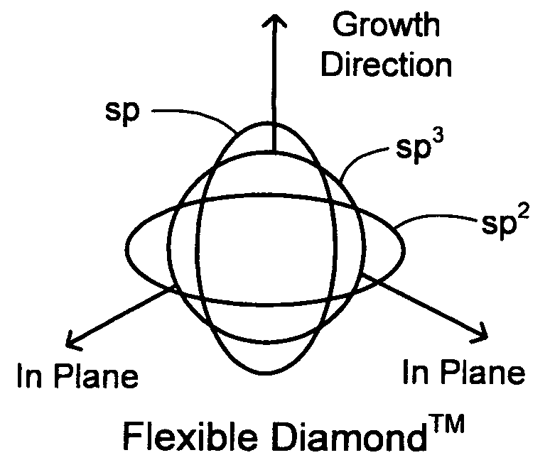
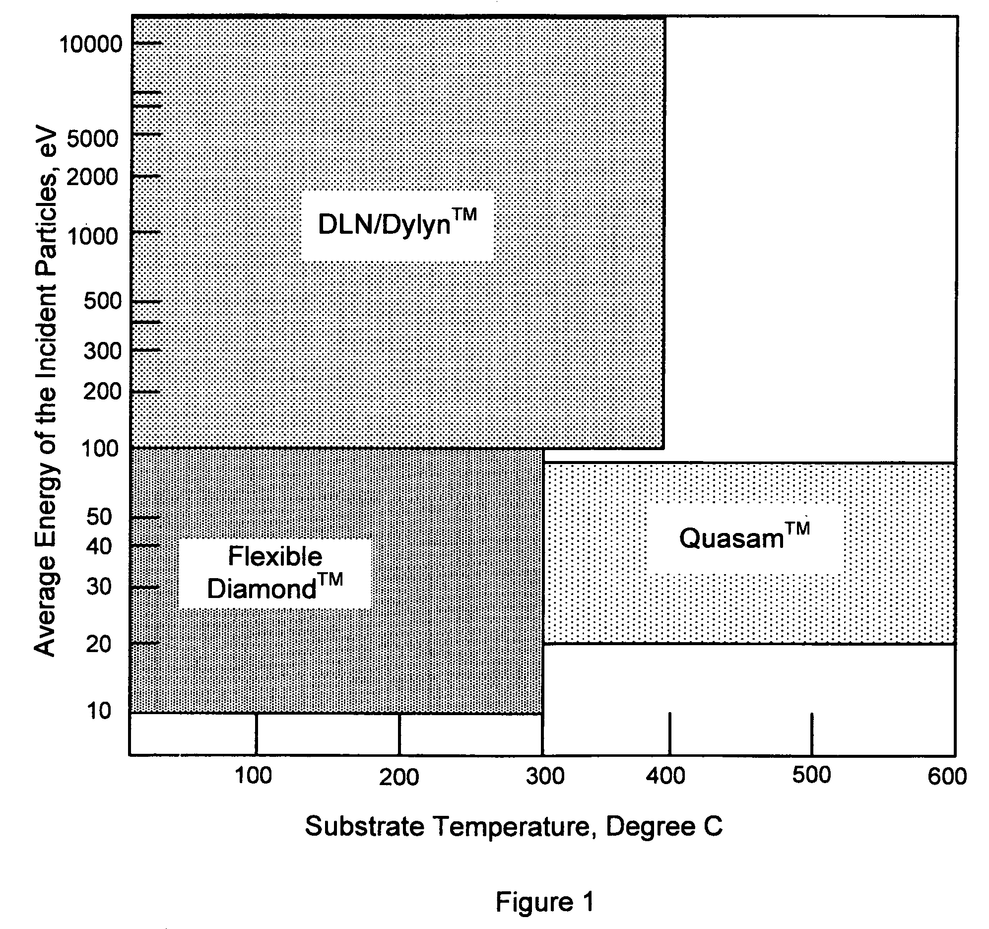
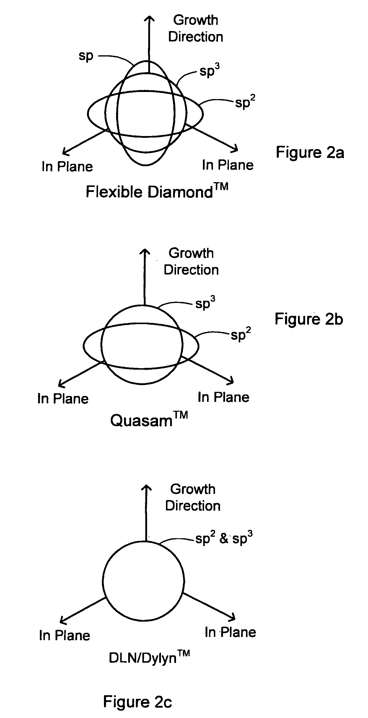
Image

Examples
example
[0056] A remote plasmatron was used to deposit a film of the present invention onto a substrate. The cathode current used was in the range of 60 to 70 A, while 65 A is typical. The plasma current used was in the range of 3 to 7 A, while 5 A is typical. The distance from the cathode to the substrate used was in the range of 10 to 30 cm, while 12 cm is typical. The initial flow rate of the liquid precursor (polysiloxane) was in the range of 2 to 6 ml / hour, while 3 ml per hour is a typical value. The pressure in the deposition chamber was maintained initially (prior to deposition process) at 1.3×10⁻² Pa. and during deposition at 5×10⁻² Pa. Note, the initial flow rate of liquid precursor may be in the range of 6 to 10 ml per hour or higher to achieve a proportionally higher growth rate of SSC material; however, this flow rate may not be preferable for depositing thin dielectric layers. The accelerating (bias) voltage precursor was 50 V (+ / −5%), frequency was 13.56 MHz, and thee substrat...
PUM
| Property | Measurement | Unit |
|---|---|---|
| density | aaaaa | aaaaa |
| dielectric constant | aaaaa | aaaaa |
| elastic modulus | aaaaa | aaaaa |
Abstract
Description
Claims
Application Information