Semiconductor device containing dielectrically isolated pn junction for enhanced breakdown characteristics

Inactive Publication Date: 2005-08-04
ALPHA & OMEGA SEMICON INC
View PDF20 Cites 114 Cited by
  • Summary
  • Abstract
  • Description
  • Claims
  • Application Information

AI Technical Summary

Benefits of technology

[0012] With this structure, depletion regions form on both sides of dielectric sidewall spacers when the MOSFET is in an off condition and blocking a voltage. This increases the avalanche breakdown voltage of the device and allows the drift region to be doped more heavily, reducing the on-resistance of the MOSFET. The dielectric spacers bordering the field shield region confi

Problems solved by technology

This increases the avalanche breakdown voltage of the device and allows the dr

Method used


Image

  • Semiconductor device containing dielectrically isolated pn junction for enhanced breakdown characteristics
  • Semiconductor device containing dielectrically isolated pn junction for enhanced breakdown characteristics
  • Semiconductor device containing dielectrically isolated pn junction for enhanced breakdown characteristics

Examples


Embodiment Construction

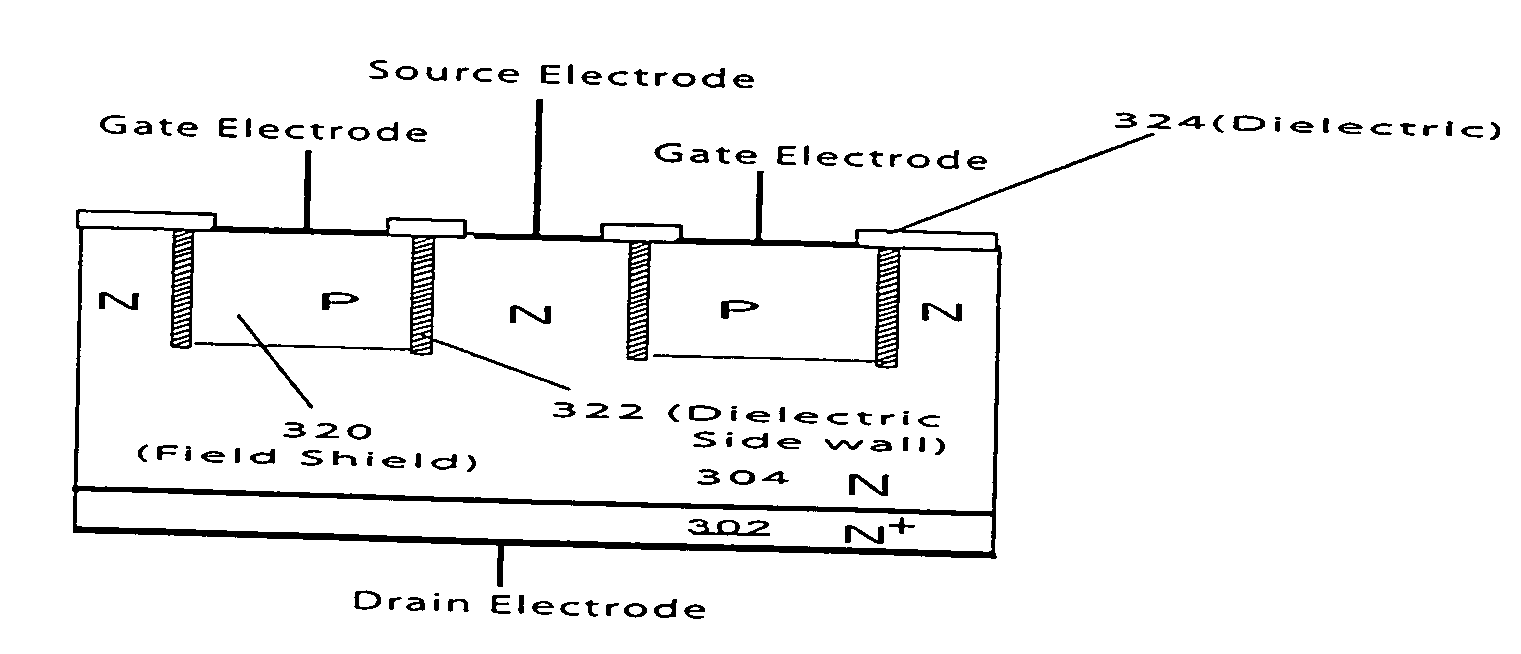
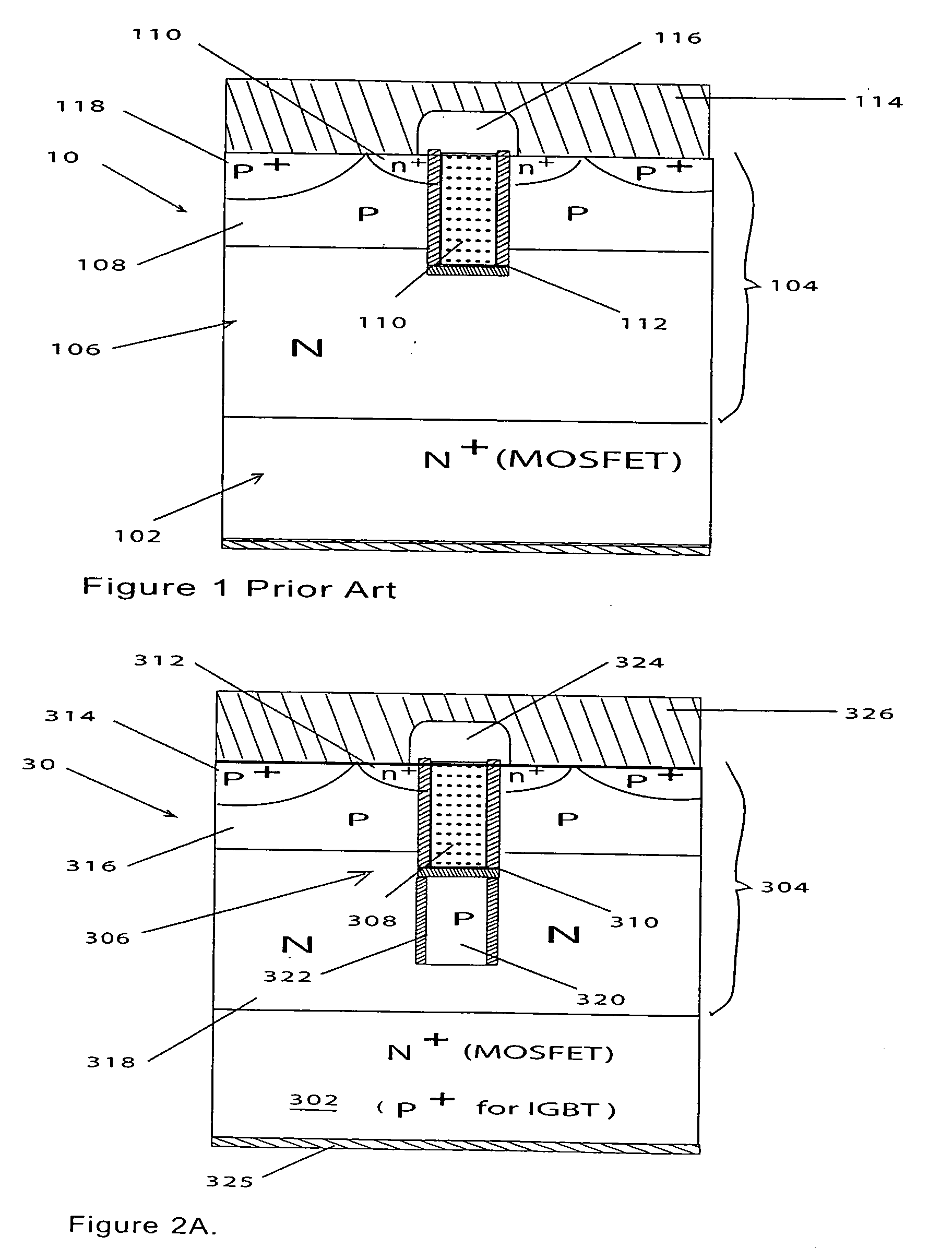
[0033]FIG. 2A shows a MOSFET 30 in accordance with this invention. MOSFET 30 is formed on an N+ substrate 302 and an overlying epi layer 304. Trenches 306 are formed in epi layer 304, and trenches 306 are lined with a gate oxide (SiO2) layer 310 and filled with agate 308. Alternatively, layer 310 could be formed of silicon nitride (Si3N4). Gate 308 is typically formed of heavily-doped polysilicon and can include a silicide.

[0034] A mesa between trenches 306 includes a P-body region 316. Within P-body region 316 are N+ source regions 312 and a P+ body contact region 314. The top surface of gate 308 is covered with a BPSG layer 324. A source metal layer 326S overlies BPSG layer 324 and makes electrical contact with N+ source regions 312 and P+ body contact regions 314. Similarly, a metal layer 325 contacts N+ substrate 302, which functions as the drain. The electrical contact between metal layer 325 and N+ substrate 302 could be ohmic or could include a Schottky barrier.

[0035] The r...


PUM


Abstract

A semiconductor device includes a field shield region that is doped opposite to the conductivity of the substrate and is bounded laterally by dielectric sidewall spacers and from below by a PN junction. For example, in a trench-gated MOSFET the field shield region may be located beneath the trench and may be electrically connected to the source region. When the MOSFET is reverse-biased, depletion regions extend from the dielectric sidewall spacers into the “drift” region, shielding the gate oxide from high electric fields and increasing the avalanche breakdown voltage of the device. This permits the drift region to be more heavily doped and reduces the on-resistance of the device. It also allows the use of a thin, 20 Å gate oxide for a power MOSFET that is to be switched with a 1V signal applied to its gate while being able to block over 30V applied across its drain and source electrodes, for example.

Description

FIELD OF THE INVENTION [0001] This invention relates to semiconductor device structures with improved packing / cell density and breakdown, and in particular MOSFETs having a gate electrode located in a trench, more specifically a low-voltage trench-gated power MOSFET having an improved breakdown characteristic, a thin gate oxide to reduce the gate drive voltage, and a high cell density to lower the on-resistance of the MOSFET. BACKGROUND OF THE INVENTION [0002] MOSFETs have become the preferred devices for switching currents in numerous fields, including the computer and automotive industries. Three of the principal characteristics of MOSFETs are their gate drive voltage, their on-resistance (Rds-on) and their avalanche breakdown voltage (VB). The gate drive voltage is determined primarily by the gate oxide thickness; the thinner the gate oxide, the lower the gate drive voltage. However, a thinner gate oxide leads to a lower breakdown voltage, especially for trench power MOSFETs. The...

Claims


Application Information

Patent Timeline
IPC IPC(8): H01L21/331H01L21/336H01L29/06H01L29/417H01L29/739H01L29/78H01L29/808H01L29/8605H01L29/872
CPCH01L29/0619H01L29/872H01L29/0634H01L29/0649H01L29/0653H01L29/1095H01L29/407H01L29/41766H01L29/456H01L29/66348H01L29/66719H01L29/66727H01L29/66734H01L29/7397H01L29/7802H01L29/7811H01L29/7813H01L29/808H01L29/8083H01L29/8605H01L29/0623
Inventor YILMAZ, HAMZA
Owner ALPHA & OMEGA SEMICON INC
Why Eureka
Try Eureka