Pre-solder structure on semiconductor package substrate and method for fabricating the same

a semiconductor package and pre-soldering technology, applied in the direction of printed circuit manufacturing, printed circuit electric connection formation, printed circuit aspects, etc., can solve the problems of reducing affecting the yield of stencil printing technology, and reducing the pitch of the conductive pad between the conductive pad and the exposed area of the solder bump, so as to prevent infiltration and bridging of the solder material, reduce the fabrication cost, and reduce the pitch of the conductive pad

Inactive Publication Date: 2005-08-04
PHOENIX PRECISION TECH CORP
View PDF5 Cites 92 Cited by
  • Summary
  • Abstract
  • Description
  • Claims
  • Application Information

AI Technical Summary

Benefits of technology

[0021] Moreover, the conductive pillars are subject to the side-etching effect that a side portion of the conductive pillar is etched away during a process to remove the seed layer by etching, such that the pad distance between the conductive pillars would be increased which can prevent migration of copper ions between the conductive pillars, and the pad pitch between the conductive pads can thus be reduced. Further, the fabrication method in the present invention can avoid the prior-art problem of a need to adjust the size of stencil openings according to the change of the size and pad pitch of conductive pads thereby leading to an increase in the fabrication cost, and the prior-art drawbacks of concerning the frequency of stencil printing and cleaning of the stencil.
[0022] Therefore, the pre-solder structure fabricated on the substrate according to the present invention desirably eliminates the prior-art drawbacks to prevent infiltration and bridging of the solder material, and also requires a reduced amount of the solder material which can shorten the fabrication time, as well as the pad pitch between the conductive pads on the semiconductor package substrate can be reduced.

Problems solved by technology

Under this condition, the area of the contact / conductive pads exposed from the solder mask layer is also reduced making the solder bumps difficult to align with and well bonded to the exposed area of the pads.
This would adversely affect the yield of the stencil printing technology and cause flash of the solder material melted during the reflow-soldering process.
Moreover, as the solder material is viscose, the more frequent performances of stencil printing leave more the solder material remaining on the inner walls of the stencil openings, which would make the amount and shape of the solder material in subsequent printing procedures not match the predetermined design.
Further, the stencil openings should be sized in accordance with the dimension of the solder mask layer, leading to an increase in the cost for fabricating the stencil.
Another difficulty may occur when a pitch between adjacent stencil openings is too small to allow the solder material to flow into the stencil openings.
Therefore, the above conventional pre-solder structure formed on the substrate suffers significant problems such as increased material cost, difficulties during the fabrication processes and degraded reliability.
Since the pitch between the conductive pads cannot be reduced, migration of copper particles and flash of the melted solder materials during reflow-soldering are caused thus leading to bridging or short circuit between two conductive pads.
However, a large amount of the solder material is required to ensure solder joints of the solder bump.
The solder material has high cost and requires longer time to be formed by electroplating as well as is not easy to be defined in location, thereby prolonging the fabrication time and increasing the fabrication complexity and cost.
However, the longer time required for electroplating the large amount of the solder material causes the solder material easy to permeate the electroplated resist layer.
And formation of the resist layer involves complex processes, thereby undesirably increasing the fabrication complexity.

Method used


Image

  • Pre-solder structure on semiconductor package substrate and method for fabricating the same
  • Pre-solder structure on semiconductor package substrate and method for fabricating the same
  • Pre-solder structure on semiconductor package substrate and method for fabricating the same

Examples


Embodiment Construction

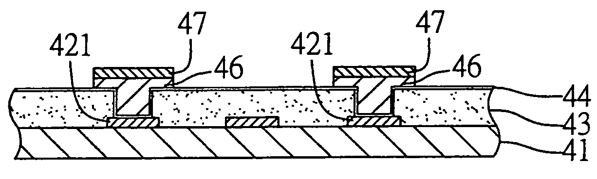
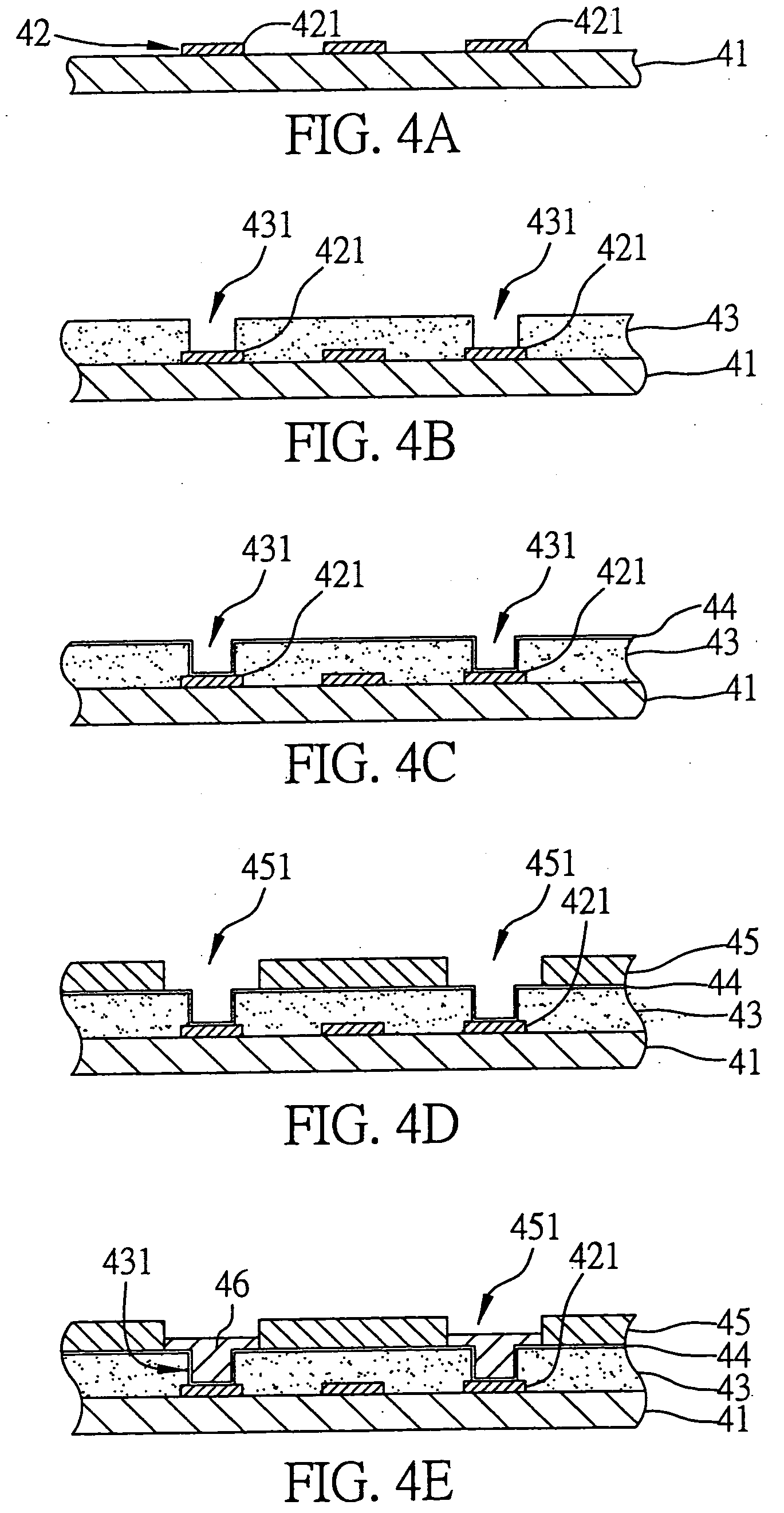
[0028] The preferred embodiments of a pre-solder structure on a semiconductor package substrate and a method for fabricating the same proposed in the present invention are described in detail with reference to FIGS. 4A to 4K.

[0029] Referring to FIG. 4A, a semiconductor package substrate 41 is provided. The substrate 41 is subject in advance to an early stage of circuit patterning to form a conductive circuit layer 42 having a plurality of conductive pads 421 on at least one surface of the substrate 41. Fabrication of the conductive circuit layer 42 and conductive pads 421 on the substrate 41 employs conventional techniques, thus not to be further detailed herein.

[0030] Referring to FIG. 4B, a protective layer 43 such as solder mask or green paint made of epoxy resign is coated on the surface of the substrate 41 having the conductive pads 421. In this embodiment, the protective layer 43 can be formed by the printing, spin-coating or attaching technique. The protective layer 43 is p...


PUM


Abstract

A pre-solder structure on a semiconductor package substrate and a method for fabricating the same are proposed. A plurality of conductive pads are formed on the substrate, and a protective layer having a plurality of openings for exposing the conductive pads is formed over the substrate. A conductive seed layer is deposited over the protective layer and openings. A patterned resist layer is formed on the seed layer and has openings corresponding in position to the conductive pads. A plurality of conductive pillars and a solder material are deposited in sequence in each of the openings. The resist layer and the seed layer not covered by the conductive pillars and the solder material are removed. The solder material is subject to a reflow-soldering process to form pre-solder bumps covering the conductive pillars.

Description

FIELD OF THE INVENTION [0001] The present invention relates to pre-solder structures on semiconductor package substrates and methods for fabricating the same, and more particularly, to a method for fabricating the pre-solder structure on conductive pads of the substrate by electroplating and etching techniques. BACKGROUND OF THE INVENTION [0002] It has been an endeavor to develop a compact semiconductor package with fine-pitch arrangement of circuits and pads. Packages having miniaturized integrated circuits (IC) and dense contacts or leads, such as BGA (ball grid array) package, flip-chip package, chip scale package (CSP) and multi-chip module (MCM), become the mainstream on the market. In the flip-chip package, a plurality of electrode pads are formed on a surface of the IC chip, and corresponding conductive pads are formed on a circuit board, such that solder bumps or other conductive adhesive material can be used to interconnect the electrode pads of the chip and the conductive ...

Claims


Application Information

Patent Timeline
Patent Type & Authority Applications(United States)
IPC IPC(8): H01L21/44H01L21/60H01L23/48H01L23/498H01L23/52H01L29/40H05K3/34H05K3/40
CPCH01L23/49816H01L2224/1147H01L2924/00013H01L2224/13609H01L2924/14H05K3/3473H05K3/4007H05K2201/0367H05K2201/09436H05K2203/043H05K2203/054H05K2203/0723H01L2224/13109H01L2224/29099H01L2224/05568H01L2224/05573H01L2224/804H01L2224/81191H01L2924/00014H01L2224/05599H01L2924/014
Inventor CHANG, RUEI-CHIHHU, CHU-CHIN
Owner PHOENIX PRECISION TECH CORP
Why Eureka
Try Eureka