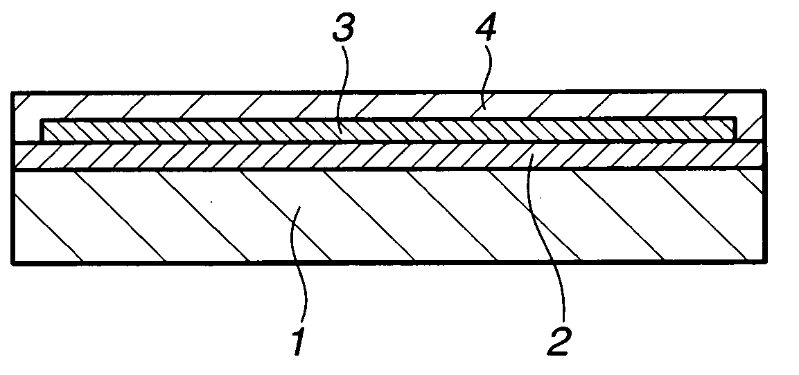
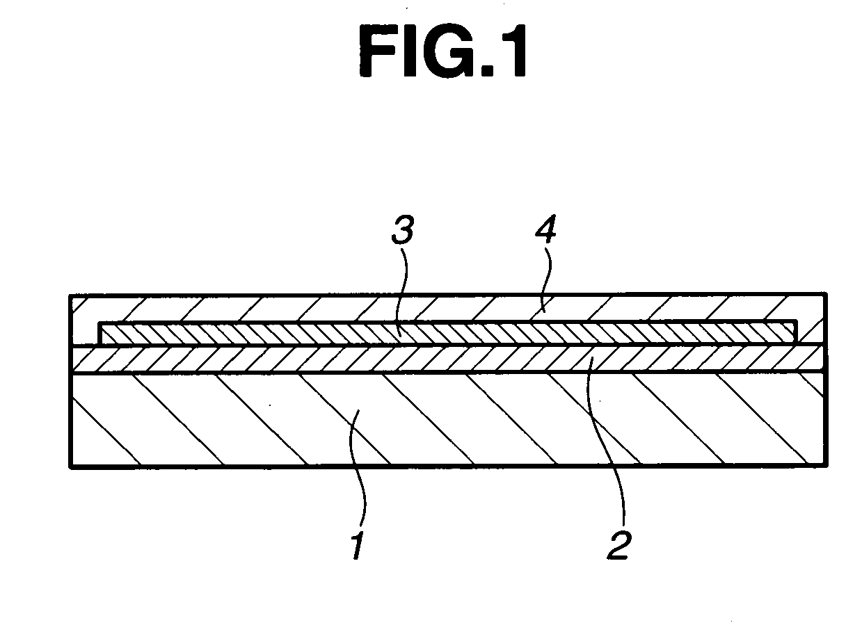
Electrostatic chuck

a technology of electrostatic chuck and chuck body, which is applied in the direction of inorganic insulators, ceramics, coatings, etc., can solve the problems of affecting so as to improve the dielectric strength, reduce the effect of etching and increase the coating thickness

Inactive Publication Date: 2005-08-04
SHIN ETSU CHEM IND CO LTD
View PDF13 Cites 17 Cited by
  • Summary
  • Abstract
  • Description
  • Claims
  • Application Information

AI Technical Summary

Benefits of technology

[0008] An object of the invention is to provide an electrostatic chuck using a high dielectric strength member bearing a sprayed coating which has both halogen plasma resistance and improved dielectric strength properties.
[0011] According to the present invention, dielectric strength is improved when a dielectric layer for an electrostatic chuck is formed using a heavy rare earth oxide having a high specific gravity preferably by an atmospheric plasma spraying. This allows a certain attractive force to be produced without increasing the coating thickness and restrains a lowering by thermal expansion of the adhesive strength between sprayed coating and substrate. The reduced thickness of coating improves the uniformity of temperature distribution within a wafer attracted thereto, thereby restraining any variation of processing on the wafer surface.

Problems solved by technology

However, alumina can be crazed and distorted when sprayed thick, giving rise to delamination and other problems.
Through the sealing treatment, organic fills are introduced into pores which in turn, become susceptible to etching, generating unwanted particles.
The increased thickness also gives rise to the problem that the adhesive strength of sprayed coating is reduced by the stresses associated with thermal expansion.

Method used


Image

  • Electrostatic chuck
  • Electrostatic chuck

Examples


example

[0029] Examples of the invention are given below by way of illustration and not by way of limitation.

examples 1-7

[0030] Sprayed coatings of 200 μm thick were formed on aluminum substrates of 100 mm×100 mm×5 mm by spraying powders of oxides of atomic number 64 to 71 rare earth elements under spraying conditions: a plasma power of 35 kW, an argon gas flow rate of 40 l / min, a hydrogen gas flow rate of 5 l / min, and a powder feed rate of 20 g / min. Without sealing treatment, the sprayed coatings were subjected to a dielectric strength test.

[0031] The dielectric strength test was performed according to JIS C2110. While the voltage was increased at a rate of 200 V / sec, the voltage at which dielectric breakdown occurred was first measured. The voltage which was lower by 0.5 kV than the breakdown voltage was then assumed to be a preset voltage. If no dielectric breakdown occurred when the voltage was increased at a rate of 200 V / sec up to the preset voltage and maintained at the preset voltage for 20 seconds, that voltage was the dielectric strength (kV) of the entire sprayed coating. The thus measured...


PUM

PropertyMeasurementUnit
dielectric strengthaaaaaaaaaa
thicknessaaaaaaaaaa
thicknessaaaaaaaaaa

Abstract

An electrostatic chuck is provided in which a lower oxide coating, an electrode, and an upper oxide coating are formed on a substrate. The lower oxide coating is formed by spraying an oxide of Gd, Tb, Dy, Ho, Er, Tm, Yb or Lu and has a dielectric strength of 15-50 kV / mm.

Description

CROSS-REFERENCE TO RELATED APPLICATION [0001] This application is a continuation-in-part of copending application Ser. No. 10 / 737,785 filed on Dec. 18, 2003, the entire contents of which are hereby incorporated by reference.BACKGROUND OF THE INVENTION [0002] 1. Field of the Invention [0003] This invention relates to an electrostatic chuck for attracting and holding a workpiece by electrostatic attraction forces and more particularly, to an electrostatic chuck as a support table for holding workpieces such as semiconductor wafers or glass substrates in the processes of manufacturing semiconductor devices and liquid crystal substrates. [0004] 2. Background Art [0005] In the conventional semiconductor manufacture process including such steps as etching of a semiconductor wafer, deposition of a thin film on a semiconductor wafer and imagewise exposure of photoresist, an electrostatic chuck is often used for holding the semiconductor wafer. [0006] One typical electrostatic chuck includes...

Claims


Application Information

Patent Timeline
Patent Type & Authority Applications(United States)
IPC IPC(8): C23C4/10B32B9/00H01B3/12H02H1/00
CPCC23C4/105C23C24/04H02H1/00C23C4/11H01B3/12
Inventor MAEDA, TAKAOSHIMA, SATOSHISHIMA, YUKO
Owner SHIN ETSU CHEM IND CO LTD
Why Eureka
Try Eureka