Bidirectional optical transceiver

a bidirectional optical transceiver and optical transceiver technology, applied in the field of optical communication, can solve the problems of reduced manufacturing yield, bulky bidirectional optical transceivers, and difficult fabrication of bidirectional optical transceivers, and achieve the effect of simple manufacturing process and compact siz

Inactive Publication Date: 2005-08-04
SAMSUNG ELECTRONICS CO LTD
View PDF13 Cites 12 Cited by
  • Summary
  • Abstract
  • Description
  • Claims
  • Application Information

AI Technical Summary

Benefits of technology

[0015] Accordingly, the present invention has been made to solve the above-mentioned problems occurring in the prior art and provides additional advantages, by providing a bidirectional optical transceiver that can be made in a compact size with a simple manufacturing process.
[0016] One aspect of the present invention is to provide a bidirectional optical transceiver having a single housing, which includes active photonic devices (e.g., an LD, a PD) and passive photonic devices (e.g., a waveguide, an optical fiber), as well as improved light source structure and optical axis alignment structure, so that it has low insertion loss and can be manufactured easily.
[0017] Another aspect of the present invention is to provide a bidirectional optical transceiver having a single housing, which includes active photonic devices (e.g., an LD, a PD) and passive photonic devices (e.g., a waveguide, an optical fiber), so that it has fewer components and has reduced manufacturing cost.

Problems solved by technology

However, conventional bidirectional optical transceivers become bulky.
Further as there are an increased number of components, the chance of a defect occurring increases and, hence, the manufacturing yield is decreased.
Such a bidirectional optical transceiver, which has manual alignment structure, is difficult to fabricate, because the photodetector, the laser diode and the optical signal monitor must be precisely aligned, typically within an error range of 1-2 μm, and fastened on the single PLC substrate.
For example, the laser diode must be fabricated so that the light exits with a very small exit angle; otherwise, high insertion loss occurs.
Further, when the laser diode is a Distributed Feedback Laser (DFB), there is no place left to include an optical isolator.
In summary, the cost of the conventional process to fabricate the optical transceiver is further increased due to the requirements for special laser diode and photodetector, and the yield is poor.

Method used


Image

  • Bidirectional optical transceiver
  • Bidirectional optical transceiver
  • Bidirectional optical transceiver

Examples


Embodiment Construction

[0027] Hereinafter, embodiment of the present invention will be described with reference to the accompanying drawings. For the purposes of clarity and simplicity, a detailed description of known functions and configurations incorporated herein will be omitted as it may make the subject matter of the present invention unclear.

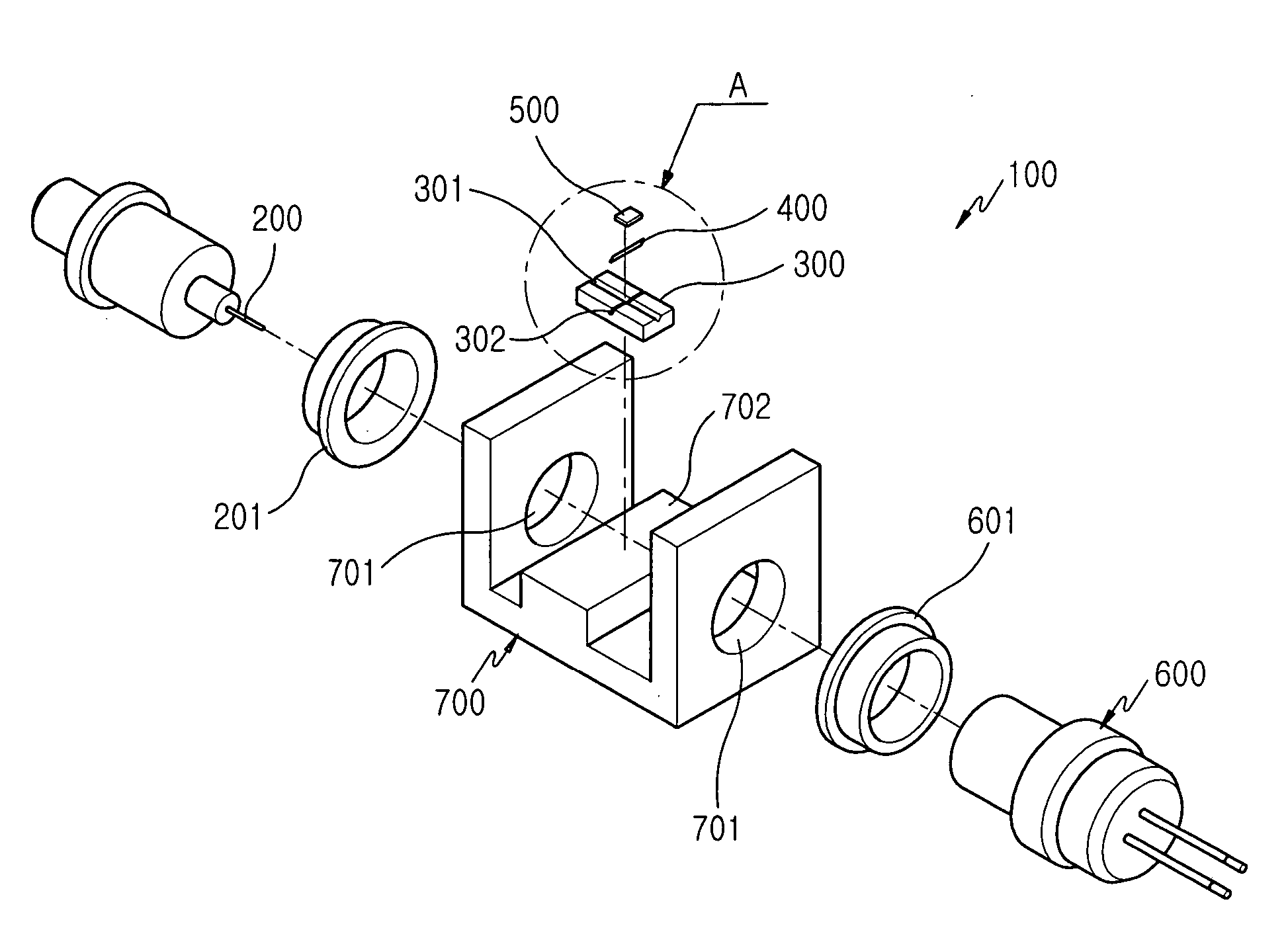
[0028]FIGS. 3-7 illustrate a bidirectional optical transceiver 100 in accordance with the principles of the invention. FIG. 3 illustrates an overview of one embodiment of bidirectional optical transceiver 100, whereas FIGS. 4-7 illustrate more detailed aspects of bidirectional optical transceiver 100.

[0029] Referring to FIG. 3, bidirectional optical transceiver 100 comprises an optical fiber 200, substrate 300, wavelength distributor filter 400, PD 500, TO-Can 600, and single housing 700. The optical fiber 200 operates to input / output optical signals 800, 900 (see FIG. 7) to / from bidirectional optical transceiver 100. Fiber 200 further includes a slant surface...


PUM


Abstract

A bidirectional optical transceiver is disclosed. The transceiver comprises an optical fiber which is adapted to input / output optical signals and has a slant surface polished with an angle, a substrate having a groove formed on its upper portion to position the optical fiber therein, a wavelength distributor filter inserted into the substrate with a slant substantially matching the angle in the optical fiber, a photodiode positioned on the substrate to receive optical signals, a TO-Can having a laser diode that is positioned in a location opposite to the optical fiber to transmit optical signals, and a single housing adapted to mount the optical fiber, the substrate, and the TO-Can thereon.

Description

CLAIM OF PRIORITY [0001] This application claims priority, pursuant to 35 USC §119, to that patent application entitled “Bidirectional Optical Transceiver,” filed with the Korean Intellectual Property Office on Feb. 4, 2004 and assigned Serial No. 2004-7371, the contents of which are hereby incorporated by reference. BACKGROUND OF THE INVENTION [0002] 1. Field of the Invention [0003] The present invention relates to an optical communications, and more particularly, to a low cost bidirectional optical transceiver having minimal component alignment criteria. [0004] 2. Description of the Related Art [0005] Generally, in optical communication utilizing optical fibers a bidirectional optical transceiver transmits a plurality of channels simultaneously using different wavelengths of light. In the case of a single-mode optical fiber, the communications typically occur at two optical wavelengths (e.g., 1.3 m and 1.55 m), because these wavelengths exhibit less attenuation. An FTTH (fiber-to-...

Claims


Application Information

Patent Timeline
Patent Type & Authority Applications(United States)
IPC IPC(8): G02B6/42H01L31/0232H01S5/022
CPCG02B6/4246G02B6/4204G02B6/4214G02B6/4215H01M6/06H01M2220/30H01M50/213Y02E60/10
Inventor PYO, SUN-HYOUNGYOON, YOUNG-KWONMUN, GI-TAERYOO, HYUN-HO
Owner SAMSUNG ELECTRONICS CO LTD
Why Eureka
Try Eureka