Methods utilizing scanning probe microscope tips and products thereof or produced thereby

Inactive Publication Date: 2005-08-11
NORTHWESTERN UNIV
View PDF9 Cites 8 Cited by
  • Summary
  • Abstract
  • Description
  • Claims
  • Application Information

AI Technical Summary

Benefits of technology

[0011] As noted above, the invention provides a method of lithography referred to as “dip pen” nanolithography, or DPN. DPN is a direct-write, nanolithography technique by which molecules are delivered to a substrate of interest in a positive printing mode. DPN utilizes a solid substrate as the “paper” and a scanning probe microscope (SPM) tip (e.g., an atomic force microscope (AFM) tip) as the “pen”. The tip is coated with a patterning compound (the “ink”), and the coated tip is used to apply the patterning compound to the substrate to produce a desired pattern. As presently understood, the molecules of the patterning compound are delivered from the tip to the substrate by capilla

Problems solved by technology

However, DPN can deliver relatively small amounts of a molecular substance to a substrate in a nanolithographic fashion that does not rely on a resist, a stamp, complicated processing methods, or sophisticated noncommercial instrumentation.
A problem that has plagued AFM since its invention is the narrow gap capillary formed between an AFM tip and sample when an experiment is co

Method used


Image

  • Methods utilizing scanning probe microscope tips and products thereof or produced thereby
  • Methods utilizing scanning probe microscope tips and products thereof or produced thereby
  • Methods utilizing scanning probe microscope tips and products thereof or produced thereby

Examples


Example

[0091] A particularly preferred nanoplotter format is described in Example 6 and illustrated in FIGS. 17 and 18. In this preferred format, a plurality of AFM tips are attached to an AFM. A multiple-tip array can be fabricated by simply physically separating an array of the desired number of cantilevers from a commercially-available wafer block containing a large number of individual cantilevers, and this array can be used as a single cantilever on the AFM. The array can be attached to the AFM tip holder in a variety of ways, e.g, with epoxy glue. Of course, arrays of tips of any spacing or configuration and adapted for attachment to an AFM tip holder can be microfabricated by methods known in the art. See, e.g., Minne et al., Applied Physics Letters, 72:2340 (1998). The plurality of tips in the array can be employed for serial or parallel DPN. When the plurality of tips is used for parallel DPN, only one of the tips needs to be connected to a feedback system (this tip is referred to...

Example

Example 1

“Dip Pen” Nanolithography With Alkanethiols On A Gold Substrate

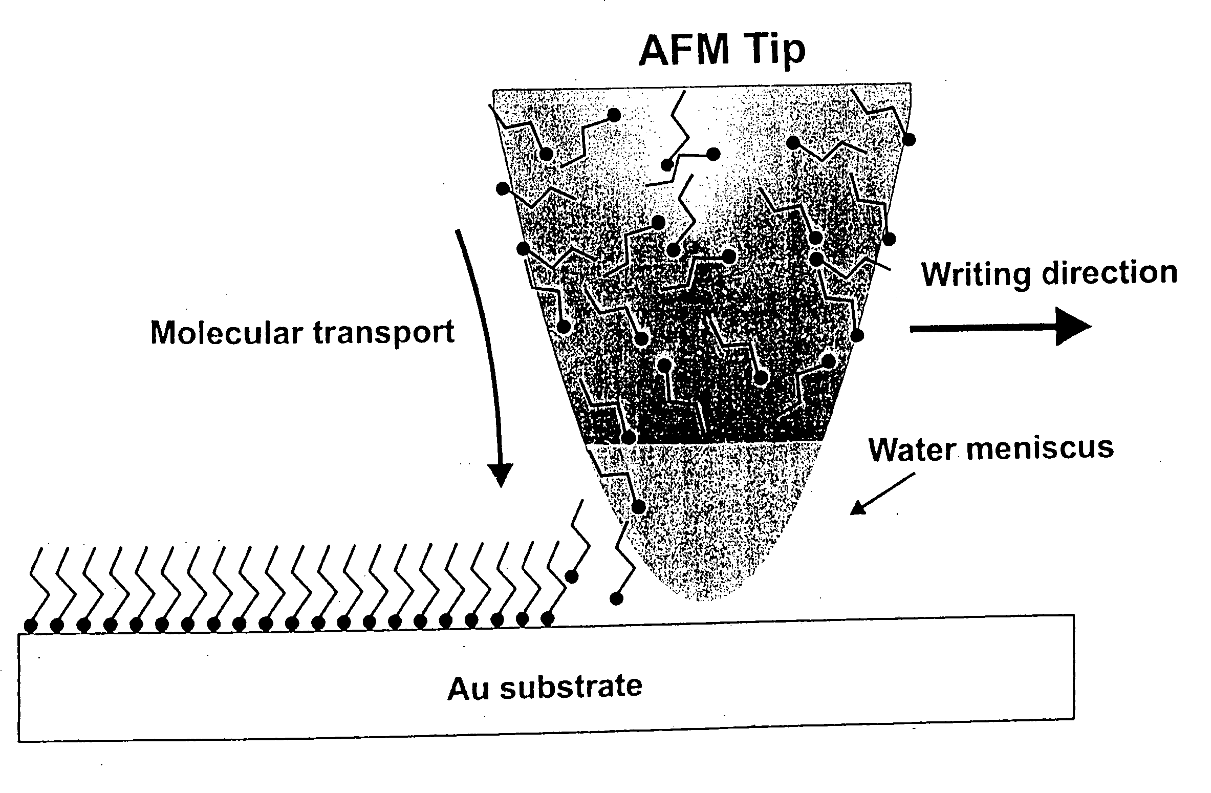
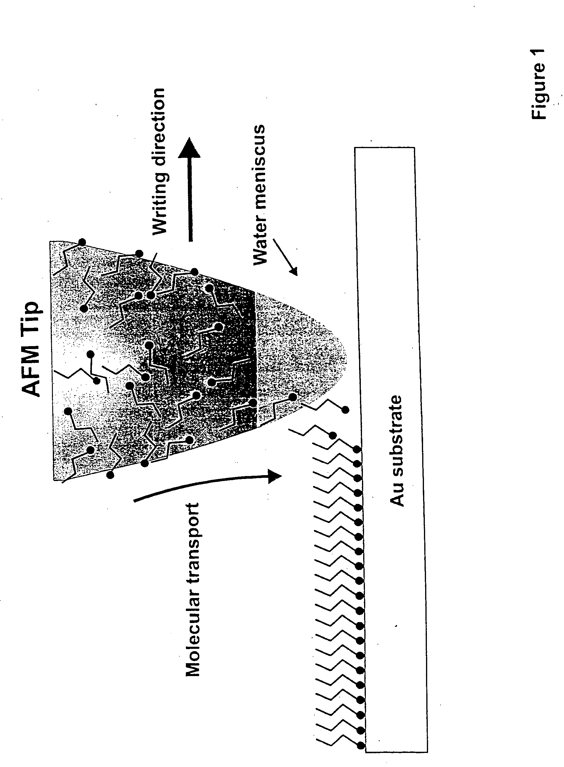
[0134] The transfer of 1-octadecanethiol (ODT) to gold (Au) surfaces is a system that has been studied extensively. See Bain et al., Angew. Chem. Int. Ed. Engl., 28:506 (1989); A. Ulman, An Introduction to Ultrathin Organic Films: From Langmuir-Blodgett to Self-Assembly (Academic Press, Boston, 1991); Dubois et al., Annu. Rev. Phys. Chem., 43:437 (1992); Bishop et al., Curr. Opin. Coll. Interf Sci., 1:127 (1996); Alves et al., J. Am. Chem. Soc. 114:1222 (1992). Au having this moderately-air-stable molecule immobilized on it can be easily differentiated from unmodified Au by means of lateral force microscopy (LFM).

[0135] When an AFM tip coated with ODT is brought into contact with a sample surface, the ODT flows from the tip to the sample by capillary action, much like a dip pen (FIG. 1). This process has been studied using a conventional AFM tip on thin film substrates that were prepared by thermally evaporat...

Example

Example 2

“Dip Pen” Nanolithography With A Variety Of Substrates And “Inks”

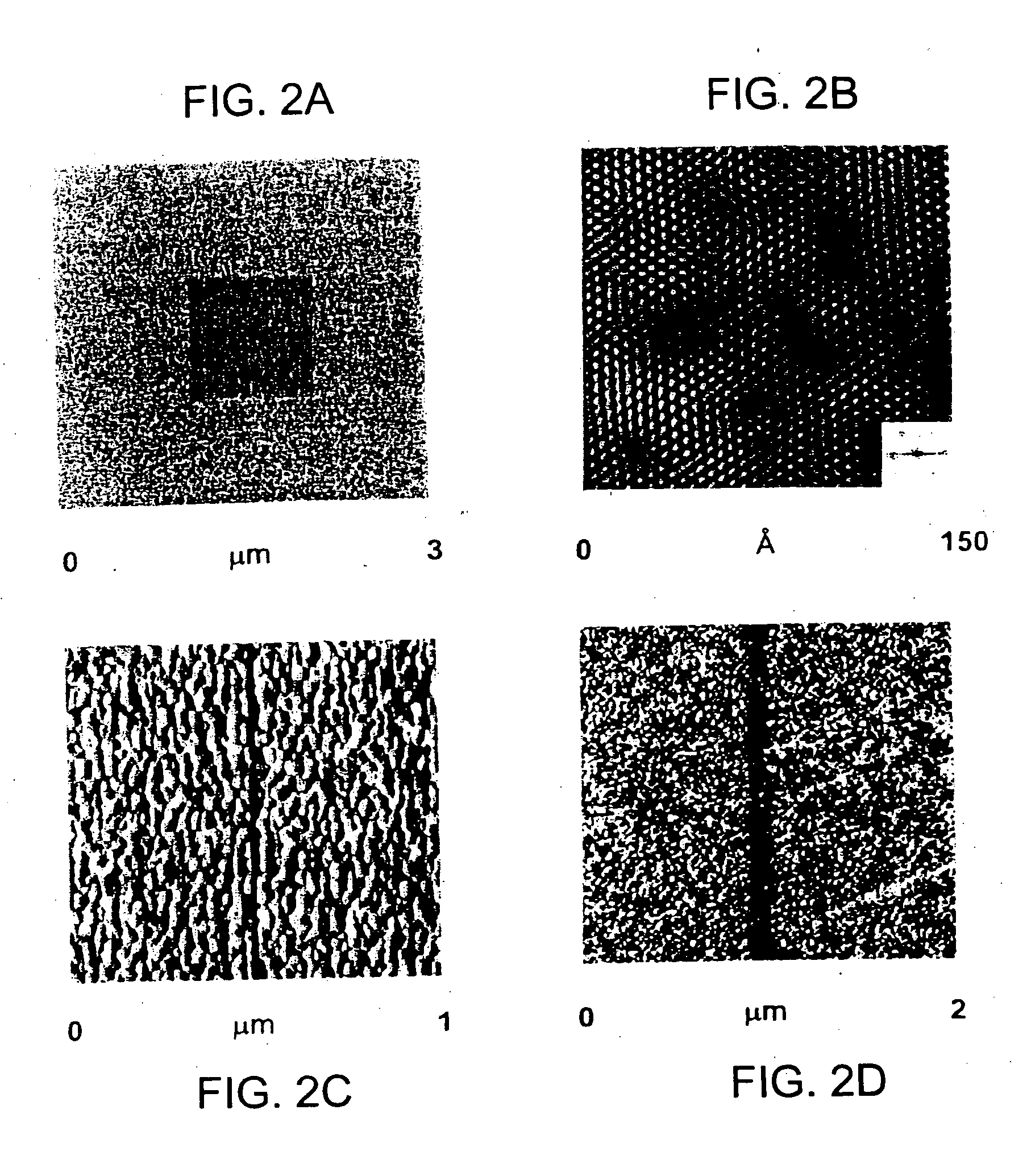
[0142] A large number of compounds and substrates have been successfully utilized in DPN. They are listed below in Table 1, along with possible uses for the combinations of compounds and substrates.

[0143] AFM tips (Park Scientific) were used. The tips were silicon tips, silicon nitride tips, and silicon nitride tips coated with a 10 nm layer of titanium to enhance physisorption of patterning compounds. The silicon nitride tips were coated with the titanium by vacuum deposition as described in Holland, Vacuum Deposition Of Thin Films (Wiley, New York, N.Y., 1956). It should be noted that coating the silicon nitride tips with titanium made the tips dull and decreased the resolution of DPN. However, titanium-coated tips are useful when water is used as the solvent for a patterning compound. DPN performed with uncoated silicon nitride tips gave the best resolution (as low as about 10 nm).

[0144] Metal film subst...


PUM


Abstract

The invention provides a lithographic method referred to as “dip pen” nanolithography (DPN). DPN utilizes a scanning probe microscope (SPM) tip (e.g., an atomic force microscope (AFM) tip) as a “pen,” a solid-state substrate (e.g., gold) as “paper,” and molecules with a chemical affinity for the solid-state substrate as “ink.” Capillary transport of molecules from the SPM tip to the solid substrate is used in DPN to directly write patterns consisting of a relatively small collection of molecules in submicrometer dimensions, making DPN useful in the fabrication of a variety of microscale and nanoscale devices. The invention also provides substrates patterned by DPN, including submicrometer combinatorial arrays, and kits, devices and software for performing DPN. The invention further provides a method of performing AFM imaging in air. The method comprises coating an AFM tip with a hydrophobic compound, the hydrophobic compound being selected so that AFM imaging performed using the coated AFM tip is improved compared to AFM imaging performed using an uncoated AFM tip. Finally, the invention provides AFM tips coated with the hydrophobic compounds.

Description

[0001] This application claims benefit of provisional applications 60 / 115,133, filed Jan. 7, 1999, 60 / 157,633, filed Oct. 4, 1999, 60 / 207,711, filed May 26, 2000, and 60 / 207,713, filed May 26, 2000, the complete disclosures of which are incorporated herein by reference. This application is also a continuation-in-part of application Ser. No. 09 / 477,997, filed Jan. 5, 2000, the complete disclosure of which is incorporated herein by reference.[0002] This invention was made with government support under grant F49620-96-1-055 from the Air Force Office Of Science Research. The government has rights in the invention.FIELD OF THE INVENTION [0003] This invention relates to methods of microfabrication and nanofabrication. The invention also relates to methods of performing atomic force microscope imaging. BACKGROUND OF THE INVENTION [0004] Lithographic methods are at the heart of modern day microfabrication, nanotechnology and molecular electronics. These methods often rely on patterning a re...

Claims


Application Information

Patent Timeline
IPC IPC(8): B05D1/00B05D1/18B05D1/26B82B3/00G01Q10/00G01Q60/00G01Q70/06G01Q70/16G01Q80/00G03F7/00G03F7/16G03F7/20H01L21/027
CPCB05D1/007Y10T428/24802B05D1/26B82B3/00B82Y10/00B82Y30/00B82Y40/00G01Q80/00G03F7/0002G03F7/165Y10S977/895Y10S977/86Y10S977/849Y10S977/857Y10S977/88Y10S977/856Y10S977/854Y10S977/853Y10S977/855Y10S977/884Y10S977/885Y10S977/886B05D1/185G21K7/00
Inventor MIRKIN, CHAD A.PINER, RICHARDHONG, SEUNGHUN
Owner NORTHWESTERN UNIV
Why Eureka
Try Eureka