Semiconductor device having bonding pad above low-k dielectric film and manufacturing method therefor
- Summary
- Abstract
- Description
- Claims
- Application Information
AI Technical Summary
Benefits of technology
Problems solved by technology
Method used
Image

Examples
first embodiment
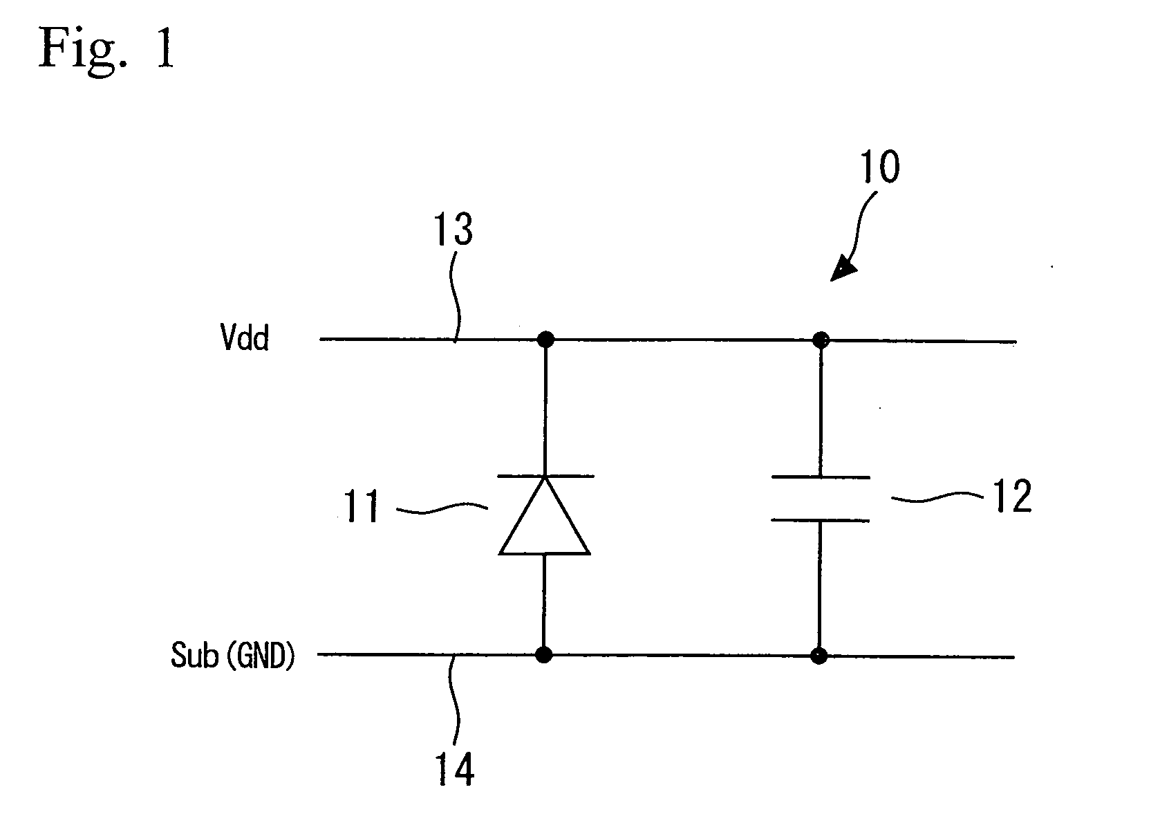
[0033] According to a first embodiment of the present invention, an explanation will be given for a case wherein a power mesh wiring structure for a protective element is also employed as a structure for reinforcing a low-k dielectric film. FIG. 1 is a circuit diagram showing a protective element according to a first embodiment of the present invention. As shown in FIG. 1, a protective element 10 in an I / O block includes a diode 11 and a capacitor element 12, both of which are connected via power supply wiring 13 to a terminal having a power voltage potential (Vdd) and are also connected via ground wiring 14 to a terminal having a ground potential (GND).
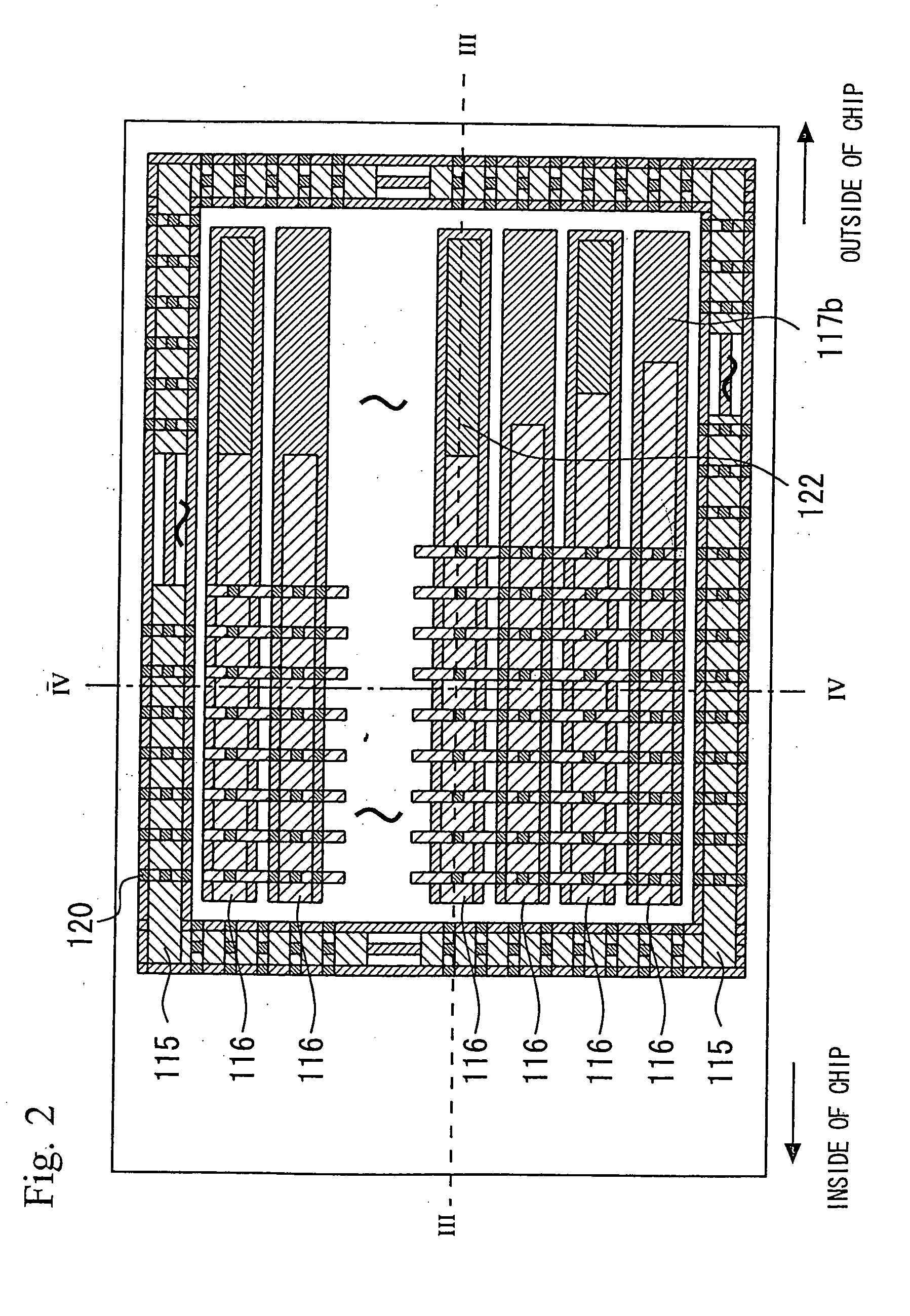
[0034]FIG. 2 is a plan view for explaining a semiconductor device according to the first embodiment, FIG. 3 is a cross-sectional view of the semiconductor device in FIG. 2 taken along line A-A′, and FIG. 4 is a cross-sectional view of the semiconductor device in FIG. 2 taken along line B-B′.
[0035] As shown in FIGS. 2 to 4, a P+ dif...
second embodiment
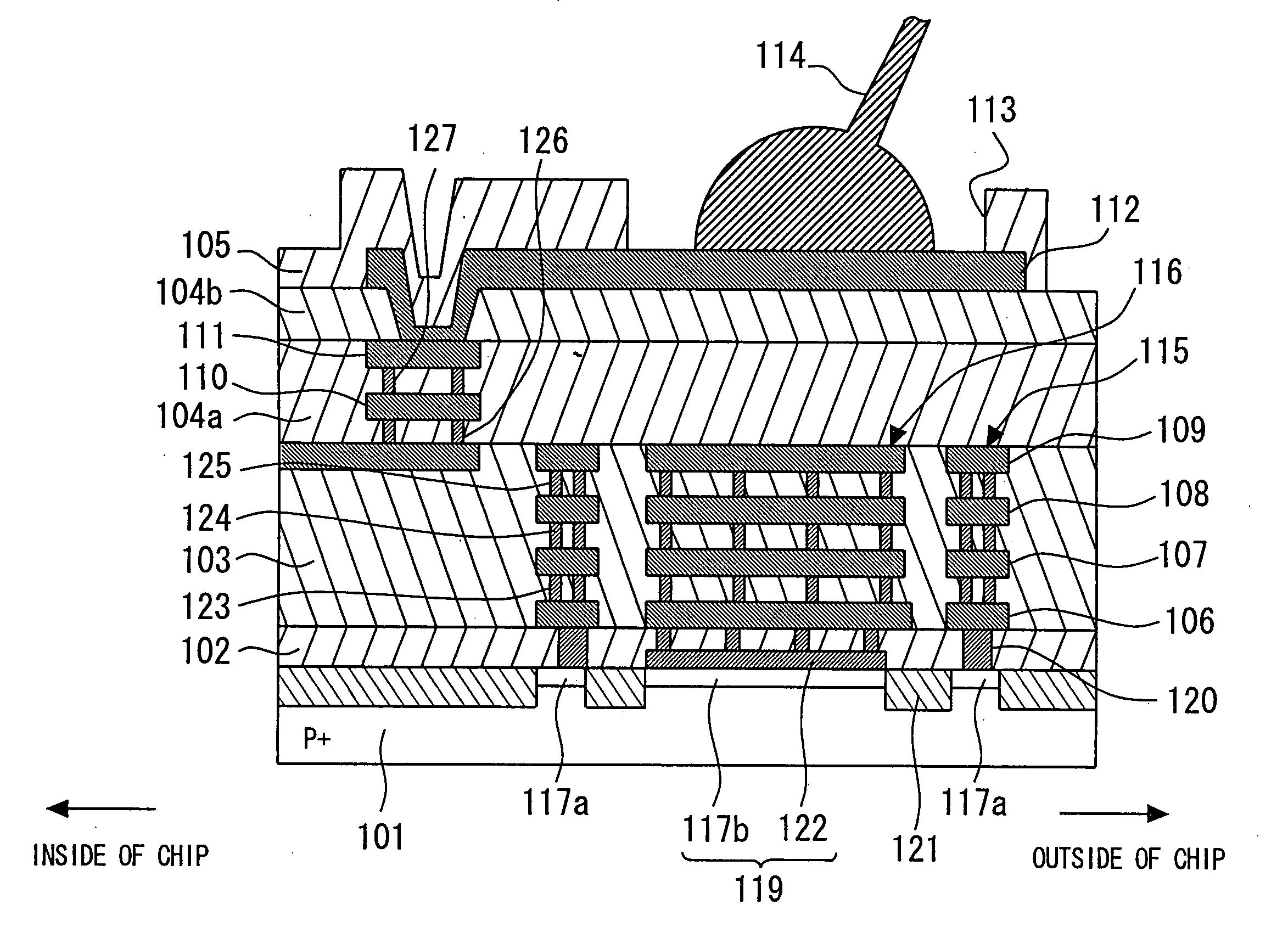
[0062] While the semiconductor device for an assembly using wire bonding has been explained in the first embodiment, a semiconductor device for a flip-chip assembly, in accordance with a second embodiment, will now be described. Mainly, the difference between this and the first embodiment will be explained.
[0063]FIG. 10 is a cross-sectional view for explaining the semiconductor device according to a second embodiment of the present invention.
[0064] As shown in FIG. 10, power supply wirings 116 are formed in the portions of a low-k dielectric film 103 above a diode 118 and a capacitor element 119, and ground wirings 115 are formed in the portions of the low-k dielectric film 103 above a diffusion layer 117a for the prevention of latch-up. The power supply wirings 116 and the ground wirings 115 for protective elements are also used as a structure for reinforcing the low-k dielectric film 103. Two silicon oxide films 114a and 114b are formed on the power supply wirings 116 and the gr...
third embodiment
[0066] For a third embodiment, an explanation will be given for a case wherein a metallic capacitor element is employed as a protective element.
[0067]FIG. 11 is a cross-sectional view for explaining a semiconductor device according to a third embodiment of the present invention, and FIG. 12 is a plan view of the power supply wiring for the semiconductor device in FIG. 11.
[0068] As shown in FIG. 12, power supply wiring 116 is formed like a comb. The comb-shaped power supply wiring 116 constitutes a metallic capacitor element. As shown in FIG. 11, the comb-shaped power supply wiring 116 is not connected to diffusion layers 117b and 118, or to a protective element such as an MIS transistor, all of which are located beneath first wiring 106. Plugs 120 are provided only in the portions of a silicon oxide film 102 beneath ground wiring 115, and the ground wiring 115 and a diffusion layer 117a are connected by the plugs 120. Since plugs are not formed in the portions of the silicon oxide...
PUM
 Abstract
Description
Claims
Application Information
 - Generate Ideas
- Intellectual Property
- Life Sciences
- Materials
- Tech Scout
- Unparalleled Data Quality
- Higher Quality Content
- 60% Fewer Hallucinations
Browse by: Latest US Patents, China's latest patents, Technical Efficacy Thesaurus, Application Domain, Technology Topic, Popular Technical Reports.
© 2025 PatSnap. All rights reserved.Legal|Privacy policy|Modern Slavery Act Transparency Statement|Sitemap|About US| Contact US: help@patsnap.com