Deep-trench 1t-sram with buried out diffusion well merged with an ion implantation well

a technology of diffusion well and deep-trench 1t-sram, which is applied in the direction of semiconductor devices, electrical devices, transistors, etc., can solve the problems of low capacitance, high fabrication cost of such prior art 1t-sram, and decreased power supply, so as to achieve lower leakage characteristics and high capacitance

Inactive Publication Date: 2005-08-25
UNITED MICROELECTRONICS CORP
View PDF4 Cites 28 Cited by
  • Summary
  • Abstract
  • Description
  • Claims
  • Application Information

AI Technical Summary

Benefits of technology

[0011] In one aspect of the present invention, the deep-trench 1T-SRAM memory cell has a buried N+ out diffusion well that is merged with the ion implantation well formed on the main surface of the substrate. The buried N+ out diffusion well and the ion implantation well serve as a capacitor plate when in operation, thereby achieving higher capacitance and lower leakage characteristics.

Problems solved by technology

Additionally, power supply has decreased.
The trend of decreasing charge storage per node makes the memory cell more susceptible to charge loss due to parasitic leakage problems.
The fabrication cost for such prior art 1T-SRAM is still high (about 4% higher than standard logic process).
Moreover, the above-said 1T-SRAM technology has severe isolation problem between two neighboring capacitors.

Method used


Image

  • Deep-trench 1t-sram with buried out diffusion well merged with an ion implantation well
  • Deep-trench 1t-sram with buried out diffusion well merged with an ion implantation well
  • Deep-trench 1t-sram with buried out diffusion well merged with an ion implantation well

Examples


Embodiment Construction

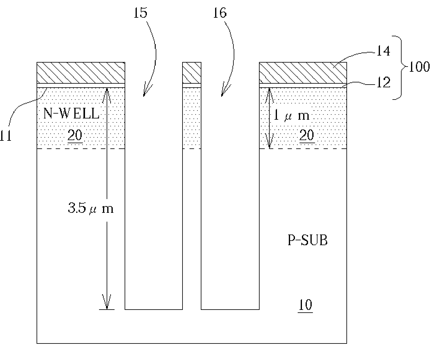
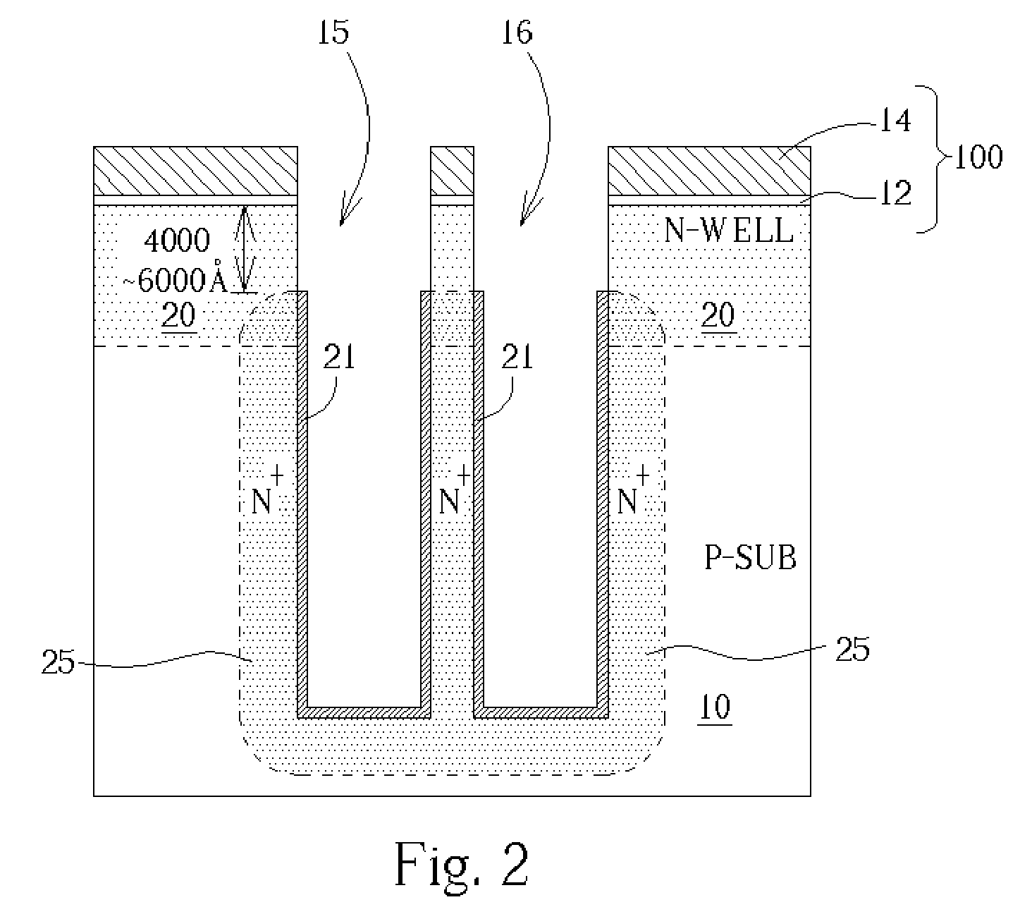
[0021] Please refer to FIG. 9. FIG. 9 is a schematic cross-sectional diagram illustrating the structure of deep-trench capacitor 1T-SRAM according to one preferred embodiment of the present invention. As shown in FIG. 9, the deep-trench capacitor 1T-SRAM cell comprises a first conductivity type semiconductor substrate 10 having a main surface 11, a second conductivity type ion implantation well 20 with a pre-determined well junction depth, say 1 micrometer, located on the main surface 11 of the semiconductor substrate 10, and a gate dielectric layer 72 formed on the ion implantation well 20. A conductive gate 81 is disposed on the gate dielectric layer 72. A first conductivity type heavily doped region 101 is disposed in the ion implantation well 20 at one side of the conductive gate 81. A lightly doped drain (LDD) region 102 of first conductivity type is disposed at the other side of the conductive gate 81 opposite to the heavily doped region 101 in the ion implantation well 20. A ...


PUM


Abstract

A deep-trench 1T-SRAM memory cell is disclosed. The deep-trench 1T-SRAM memory cell includes a first conductivity type semiconductor substrate with a main surface. A second conductivity type ion implantation well with a well junction depth is located on the main surface. A gate dielectric layer is located on the ion implantation well. A gate is located on the gate dielectric layer. A heavily doped S / D region of the first conductivity type is disposed at one side of the gate in the ion implantation well. A lightly doped drain (LDD) region of the first conductivity type is disposed at the other side of the gate in the ion implantation well. A deep trench capacitor vertically extends into the main surface through the well junction depth of the ion implantation well to a pre-selected depth. The deep trench capacitor, which is fabricated adjacent to the LDD region, comprises an ion out diffusion well of the second conductivity type that is formed at a lower portion of the deep trench capacitor and is merged with the ion implantation well. A polysilicon electrode pillar is electrically isolated from the LDD region, the ion implantation well, and the ion out diffusion well by a capacitor dielectric layer and a trench top insulation layer.

Description

BACKGROUND OF INVENTION [0001] 1. Field of the Invention [0002] The present invention relates to the field of deep-trench semiconductor memory devices, and more particularly, to a deep-trench one-transistor static random access memory (1T-SRAM) device and fabrication method thereof. [0003] 2. Description of the Prior Art [0004] Semiconductor memory devices such as random access memory (RAM) devices typically include a number of memory cells coupled to at least one bit line. The memory cells often include at least one storage device, storage node, and pass gate transistor. Generally, in a static random access memory (SRAM) cell, two storage devices such as drive transistors are coupled between two pass gate transistors, and a bit line is coupled to each of the pass gate transistors. Thus, each memory cell is often located between two bit lines. The pass gate transistors (e.g., transfer gates) have gate electrodes that are coupled to word lines. A signal such as an address or select s...

Claims


Application Information

Patent Timeline
Patent Type & Authority Applications(United States)
IPC IPC(8): H01L21/8242H01L21/8244H01L27/108H01L27/11
CPCH01L27/11H01L27/10861H10B12/038H10B10/00
Inventor CHENG, CHUN-WEN
Owner UNITED MICROELECTRONICS CORP
Why Eureka
Try Eureka