Non-volatile memory device having a charge storage oxide layer and operation thereof

a non-volatile memory and oxide layer technology, applied in the direction of semiconductor devices, basic electric elements, electrical appliances, etc., can solve the problems of high power consumption, complex peripheral circuits, and all charges stored in floating gate storage may be lost, so as to improve program and erase efficiency, simplify formation process, and improve productivity

Inactive Publication Date: 2005-08-25
SAMSUNG ELECTRONICS CO LTD
View PDF6 Cites 8 Cited by
  • Summary
  • Abstract
  • Description
  • Claims
  • Application Information

AI Technical Summary

Benefits of technology

[0011] It is another feature of an embodiment of the present invention to provide a non-volatile memory device having a simplified formation processes, thereby improving productivity...

Problems solved by technology

A volatile memory device, e.g., a dynamic random access memory (DRAM), needs a refresh operation to retain data, resulting in high power consumption.
Since the floating gate type memory device uses a conductive floating gate as a charge storage layer, if a defect occurs on a part of a tunnel oxide layer separating the floating gate and a semiconductor substrate, all charges stored in the floating gate may be lost.
As the thickness of the tunnel oxide lay...

Method used


Image

  • Non-volatile memory device having a charge storage oxide layer and operation thereof
  • Non-volatile memory device having a charge storage oxide layer and operation thereof
  • Non-volatile memory device having a charge storage oxide layer and operation thereof

Examples


first embodiment

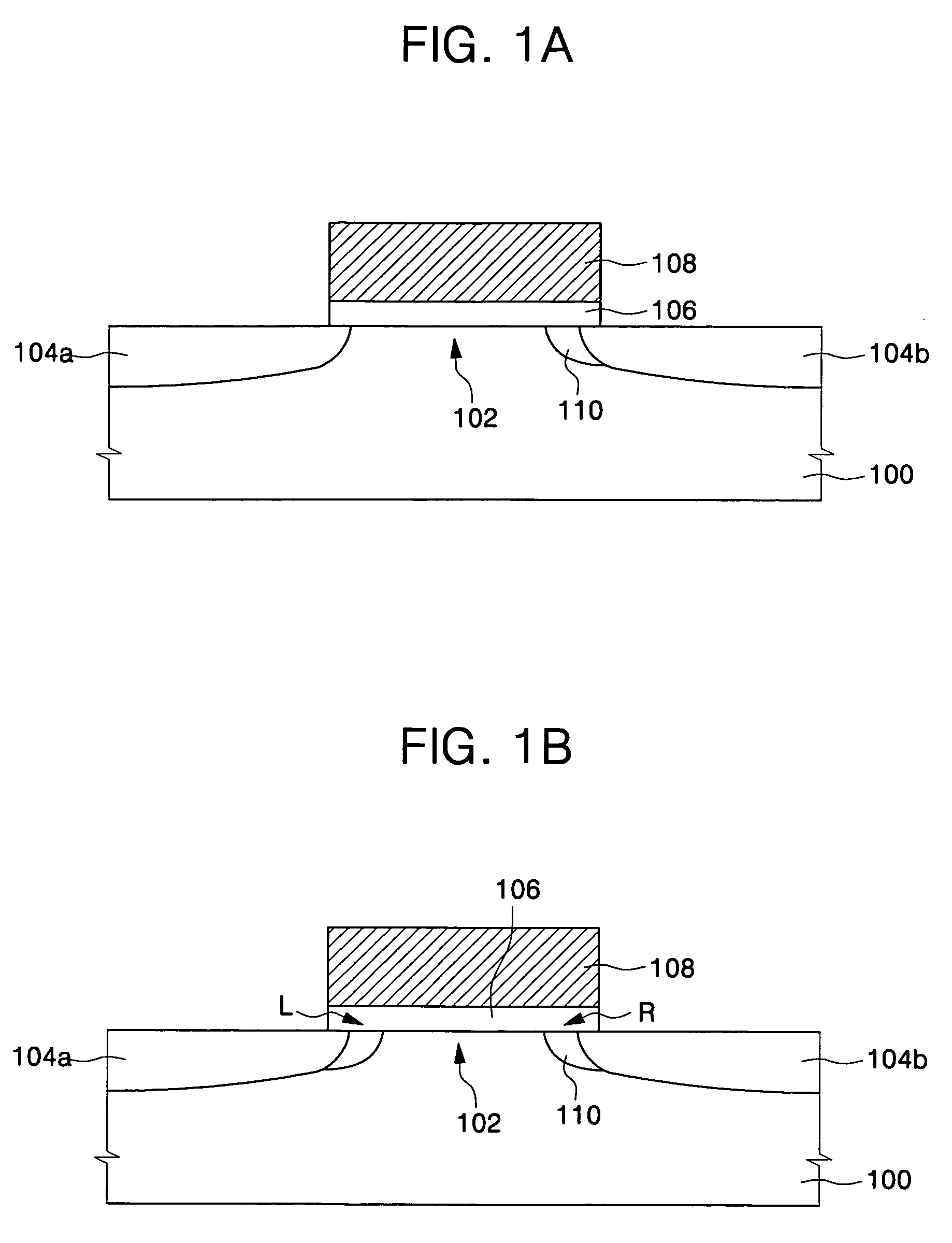
[0030]FIGS. 1A and 1B illustrate cross-sectional views of a non-volatile memory device according to the present invention.

[0031] Referring to FIGS. 1A and 1B, a pair of source / drain regions 104a, 104b, which are spaced apart from each other by a channel region 102, are disposed in a semiconductor substrate 100 having a first conductivity. The source / drain regions 104a, 104b are diffusion regions of impurity ions having a second conductivity. A charge storage oxide layer 106 is disposed on the channel region 102. The charge storage oxide layer 106 overlaps a part of the source / drain regions 104a, 104b.

[0032] The charge storage oxide layer 106 may be formed of one layer selected from the group consisting of a silicon oxide (SiO2) layer, a silicon oxynitride (SiON) layer, an aluminum oxide (Al203) layer, a zirconium oxide (ZrO2) layer, a hafnium oxide (HfO2) layer, a lanthanum oxide (La2O5) layer, and a stacked layer including any combination thereof. The charge storage oxide layer 10...

second embodiment

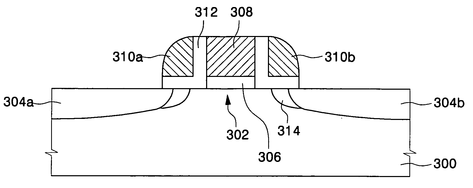
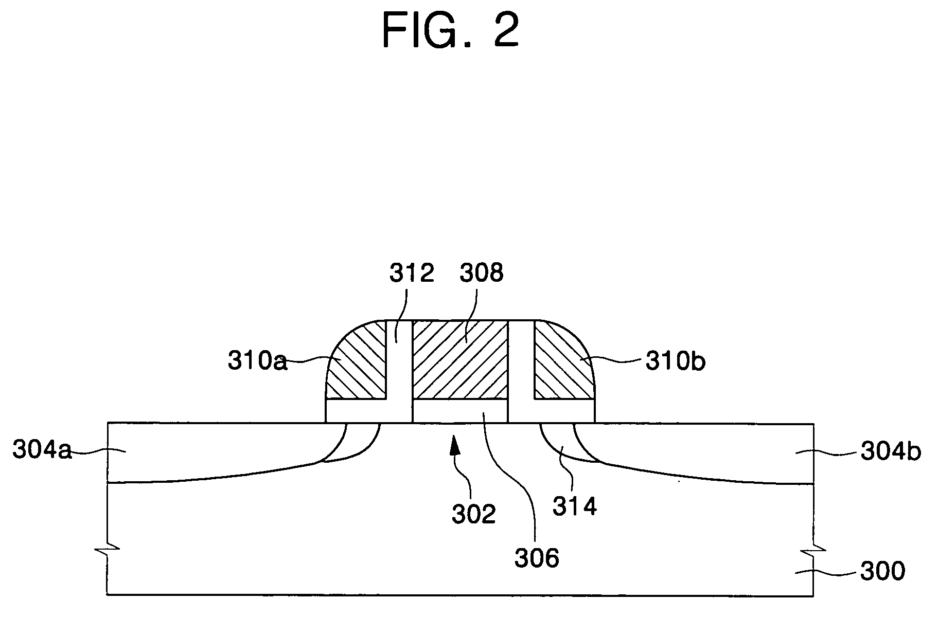
[0048]FIG. 2 illustrates a cross-sectional view of a non-volatile memory device according to the present invention.

[0049] Referring to FIG. 2, a pair of source / drain regions 304a, 304b, which are spaced apart from each other by a channel region 302, are disposed in a semiconductor substrate 300 having a first conductivity. The pair of source / drain regions 304a, 304b have a second conductivity. A main gate insulating layer 306 and a main gate electrode 308 are sequentially stacked on the channel region 302, and spaced apart from the pair of the source / drain regions 304a, 304b. The main gate insulating layer 306 may be a thermal oxide layer. Further, the main gate electrode 308 may be formed of poly silicon. Sidewall gate electrodes 310a, 310b are disposed on both sidewalls of the main gate electrode 308, and overlap a part of the source / drain regions 304a, 304b. The sidewall gate electrodes 310a, 310b may be poly silicon. Charge storage oxide layers 312 are continuously interposed be...


PUM


Abstract

A non-volatile memory device includes a pair of source/drain regions disposed in a semiconductor substrate, having a channel region between them. A charge storage oxide layer is disposed on the channel region and overlaps part of each of the pair of source/drain regions. A gate electrode is disposed on the charge storage oxide layer. At least one halo implantation region is formed in the semiconductor substrate adjacent to one of the pair of source/drain regions, and overlapping the charge storage oxide layer. A program operation is performed by trapping electrons in the charge storage oxide layer located near the source/drain region where the halo ion implantation region is formed, and an erase operation is performed by injecting holes into the charge storage oxide layer located near the source/drain region where the halo ion implantation region is formed.

Description

BACKGROUND [0001] 1. Field of the Invention [0002] The present invention relates to a non-volatile memory device. More particularly, the present invention relates to a non-volatile memory device having a charge storage oxide layer and operation thereof.[0003] 2. Description of Related Art [0004] In contrast to a volatile memory device, a non-volatile memory device retains data stored in its memory cells even with supplied power turned off. A volatile memory device, e.g., a dynamic random access memory (DRAM), needs a refresh operation to retain data, resulting in high power consumption. In contrast, a non-volatile memory device, e.g., a flash memory / electrical erasable programmable read only memory (EEPROM), has a large capacity, low power consumption, and typically used for a file system, a memory card, a portable appliance, etc. [0005] Generally, non-volatile memory devices are classified into a floating gate type memory device and a floating trap type memory device, depending on ...

Claims


Application Information

Patent Timeline
IPC IPC(8): H01L27/115H01L21/28H01L21/336H01L21/8242H01L29/792
CPCH01L21/28282H01L29/7923H01L29/792H01L29/66833H01L29/40117
Inventor KIM, KI-CHULBAE, GEUM-JONGLEE, BYOUNG-JINKIM, SANG-SU
Owner SAMSUNG ELECTRONICS CO LTD
Why Eureka
Try Eureka