Self-masking defect removing method

a defect removal and defect technology, applied in the field of self-masking defect removal, can solve the problems of growth defects on the surface, adversely affecting the ability to join surfaces, and negatively affecting the yield of integrated circuit fabrication, and achieve the effect of simple wafer surface cleaning

Inactive Publication Date: 2005-08-25
HRL LAB
View PDF6 Cites 17 Cited by
  • Summary
  • Abstract
  • Description
  • Claims
  • Application Information

AI Technical Summary

Benefits of technology

[0012] Embodiments of the present invention provide a method which improves the surface morphology of epitaxial layers grown on semiconductor wafers for applications in wafer bonding or integrated circuit fabrication. Defective regions or localized defect structures are locally removed from the wafer surface by employing a self-masking process that confines an etching process to the defected area.
[0015] The method is generally applicable to all semiconductor materials, can be performed as a low-cost batch process and, being a non-mechanical process, does not affect the good portions of the wafer. Additionally, the method according to the present invention allows a simple clean up of the wafer surface for subsequent wafer bonding or IC fabrication processes.

Problems solved by technology

Growth defects on the surface of a semiconductor wafer are typically generated during the growth of epitaxial layers or epilayers and are the result of effusion cell spitting during molecular beam epitaxy or from interference during the growth of the epilayer due to impurities on the surface of the substrate or incomplete oxide desorption from the surface of the substrate prior to growth.
The defects are known to adversely affect the ability to join surfaces by wafer bonding and negatively affect the yield of integrated circuit fabrication.
In particular, in the case of wafer bonding, protruding defects cause the bonding wafers to deform around them forming circularly unbonded interface areas or voids.
CMP has a number of disadvantages when applied to the removal of growth defects from epilayers.
A first disadvantage is due to the inadvertent thinning of critical thickness epilayers during the defect removal process.
A second disadvantage is the need of cleaning the polished wafer surface after applying the slurry.
A third disadvantage is due to the non-uniform etching of the wafer surface due to the random positions of the defects.
A first disadvantage of this process is that suitable RIE etching chemistries must be found for each defect material and sacrificial layer combination.
A second disadvantage of this process is that a complete removal of defects from the structures requires etching of the entire epilayer surface that may result in surface roughening or partial removal of the thin epilayers.
The drawbacks of the above mentioned direct planarization techniques also depend on the kind and distribution of the defects on the surface of a semiconductor wafer.
Such defects typically range in size from 1-100 microns and in densities from 1-100 / cm2 and are non-uniformly distributed over the wafer surface.
Other possible techniques such as serial etching methods (FIB, laser ablation, etc) are too expensive or time-intensive for the large numbers and random distribution of the defects.

Method used


Image

  • Self-masking defect removing method
  • Self-masking defect removing method
  • Self-masking defect removing method

Examples


first embodiment

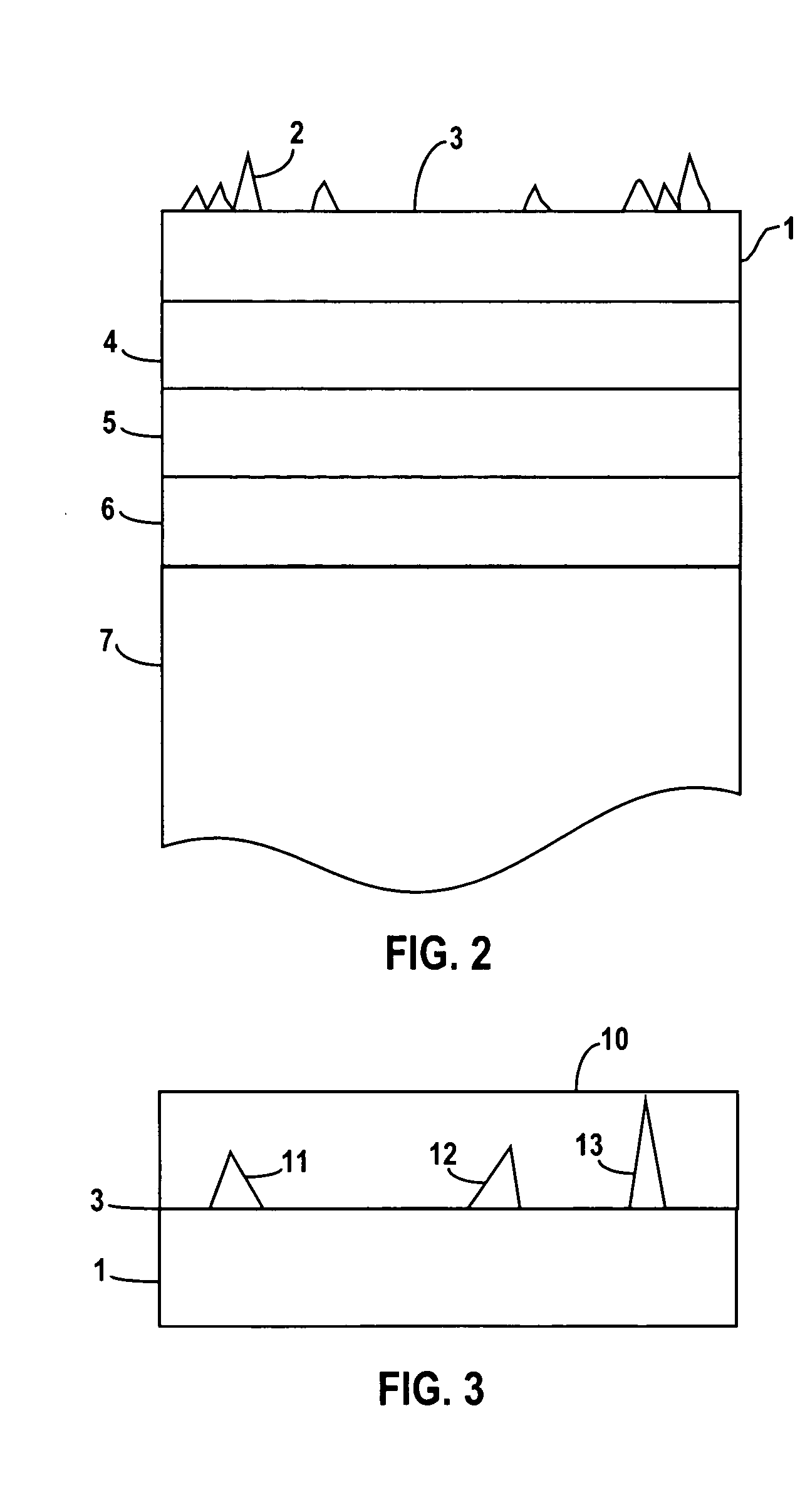
[0022] According to the first step, the coating layer 10 comprises a photoresist layer. It is preferable that the height of the photoresist layer exceeds the height of the defects to ensure that the resulting surface is planar, in order to enable defects to be successfully revealed during a subsequent thinning process. Generally, for epilayers on GaSb and InAs substrates, the photoresist layer has a thickness from about 5 to about 10 microns and preferably of about 8 microns. This thickness is usually sufficient to uniformly cover all defects.

second embodiment

[0023] According to the first step, the coating layer 10 comprises a deposited silicon oxide film or a deposited silicon nitride film having, for example, a thickness from about 1000 to about 6000 Angstrom. Oxide and nitride films can be deposited using a plasma enhanced chemical vapor deposition (PECVD) system at 100-300° C. and are controlled to yield low stress films on the host wafer.

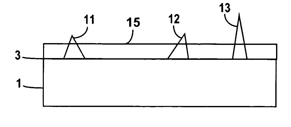
[0024]FIG. 4 shows a second step of the method, where the protective layer 10 is thinned to form a thinned protective layer 15. The thinning step allows to selectively reveal portions of the protruding defective structures 11, 12, and 13, at the same time protecting the remainder of the surface 3 of the semiconductor 1. For example, in order to reveal defects having a height larger than 0.5 microns, the photoresist layer can be thinned to 0.5 microns.

[0025] In the photoresist layer embodiment, thinning is preferably accomplished using an Inductively Coupled Plasma (ICP) oxygen process that enables ...


PUM

PropertyMeasurementUnit
thicknessaaaaaaaaaa
thicknessaaaaaaaaaa
thicknessaaaaaaaaaa

Abstract

A method for removing defects from a semiconductor surface is disclosed. The surface of the semiconductor is first coated with a protective layer, which is later thinned to selectively reveal portions of the protruding defects. The defects are then removed by etching. Finally, also the protective layer is removed. According to the method, inadvertent thinning of the surface is prevented and removal of the defects is obtained.

Description

BACKGROUND [0001] 1. Field [0002] The present invention is generally related to semiconductor technology and, more particularly, is related to a method for removing defects from a surface of a semiconductor wafer without affecting the surrounding non-defective regions of the semiconductor wafer. [0003] 2. Related Prior Art [0004] Growth defects on the surface of a semiconductor wafer are typically generated during the growth of epitaxial layers or epilayers and are the result of effusion cell spitting during molecular beam epitaxy or from interference during the growth of the epilayer due to impurities on the surface of the substrate or incomplete oxide desorption from the surface of the substrate prior to growth. Such unwanted defects are an integral part of the semiconductor wafer surface and are composed of the same material as the surrounding active device layers. See, for example, E. H. C. Parker, “The Technology and Physics of Molecular Beam Epitaxy” pages 90-93, Plenum Press ...

Claims


Application Information

Patent Timeline
Patent Type & Authority Applications(United States)
IPC IPC(8): H01L21/02H01L21/306H01L21/308H01L21/3105H01L21/461
CPCH01L21/02052H01L21/30612H01L21/30604
Inventor BREWER, PETER D.
Owner HRL LAB
Why Eureka
Try Eureka