III-nitride device and method with variable epitaxial growth direction

Active Publication Date: 2005-09-01
INFINEON TECH AMERICAS
View PDF6 Cites 7 Cited by
  • Summary
  • Abstract
  • Description
  • Claims
  • Application Information

AI Technical Summary

Benefits of technology

[0013] In accordance with an advantage of the present invention, a semiconductor device obtained through the growth techniques described herein obtains significant advantages over ion implantation vertical devices, as well as horizontal base devices. Advantageously, breakdown voltage is increased due to the elimination of damage caused by ion implantation. Furthermore, the resulting devices have an increased current carrying capacity for a given voltage rating due to the higher carrier density in the voltage standoff region. The unique geometries permitted by the techniques of the present invention permit higher performance in comparable devices due to, for example, charge compensation in the vertical base.
[0014] According to another advantage of the present invention, a vertical base may be fabricated without etching and regrowth, as is traditionally done i

Problems solved by technology

The implantation of ions according to these typical techniques often involve high energy collisions between the implanted ions and the lattice structure of the semiconductor material to be implanted.
Accordingly, structural damage to the lattice of the semiconductor material is a typical and well known byproduct of the doping process.
However, as more complicated implantation processes are conducted, a significant amount of structural damage to the implanted semiconductor materi

Method used


Image

  • III-nitride device and method with variable epitaxial growth direction
  • III-nitride device and method with variable epitaxial growth direction
  • III-nitride device and method with variable epitaxial growth direction

Examples


Example

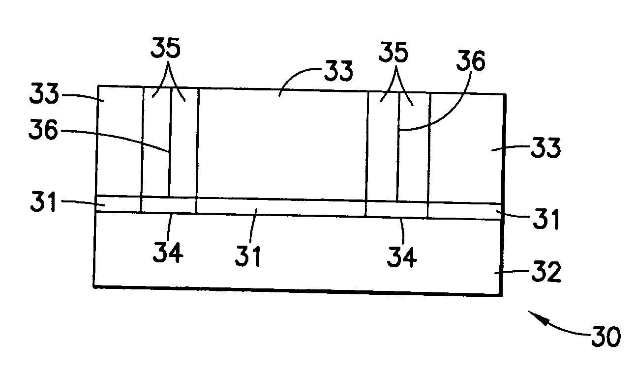
[0019] Referring now to FIG. 1, an exemplary embodiment of an epitaxially grown vertical based III-nitride device 10 is illustrated. Device 10 is a bipolar MOS transistor. It is a vertical conduction device with ohmic contacts 12, 13 providing high current connections to device 10. Contacts 12, 13 are typically thought of as source and drain contacts, respectively. In MOSgated silicon devices, however, such a naming convention should not be construed to mean that device 10 is a unipolar device, or is operable in a single direction. Accordingly, contacts 12, 13 are referred to as ohmic contacts, or source / drain contacts interchangeably without limitation to the conduction direction or carriers used in device 10.

[0020] Device 10 includes a substrate 15 composed of a suitable material such as silicon, silicon carbide, III-nitride materials and so forth. Substrate 15 may be etched or grown to form trenches 17. A dielectric or protective layer 19 overlays substrate 15, and can be used a...


PUM


Abstract

A semiconductor device composed of III-nitride materials is produced with epitaxial growth that permits vertical and lateral growth geometries to improve device characteristics. The resulting device has a greater breakdown voltage due to the greater integrity of the semiconductor material structure since no ion implantation processes are used. The epitaxially grown layers also exhibit greater thermal conductivity for improved operation with power semiconductor devices. The device may include a laterally grown charge compensated area to form a superjunction device. The resulting device may be bidirectional and have improved breakdown voltage in addition to higher current capacity for a given voltage rating.

Description

RELATED APPLICATION [0001] The present application is based on and claims benefit of U.S. Provisional Application No. 60 / 527,626, filed Dec. 5, 2003, entitled Epitaxially Grown Vertical Base Bipolar MOS Transistor, to which a claim of priority is hereby made, and the disclosure of which is incorporated herein by reference.BACKGROUND OF THE INVENTION [0002] 1. Field of the Invention [0003] The present invention relates generally to the construction of III-nitride devices using epitaxial growth, and relates more particularly to the construction of III-nitride devices where the epitaxial growth is variable in direction to obtain variable doping profiles without implantation. [0004] 2. Description of Related Art [0005] In the construction of semiconductor devices, doping of various portions of semiconductor material is achieved according to a number of different techniques. One of the more popular techniques is the implantation of ions using a beam, and driving the implanted impurities ...

Claims


Application Information

Patent Timeline
IPC IPC(8): H01L21/331H01L21/76H01L29/20
CPCH01L29/66325H01L29/2003
Inventor BEACH, ROBERTBRIDGER, PAUL
Owner INFINEON TECH AMERICAS
Why Eureka
Try Eureka