
Optical semiconductor device

a semiconductor and optical technology, applied in semiconductor lasers, printed circuit aspects, printed circuit non-printed electric components association, etc., can solve the problems of high stress to be developed at the soldered portion of the circuit board, damage, unsoldering, etc., to reduce the distortion of waveforms and restrain interference of high frequencies.

Active Publication Date: 2005-09-08
MITSUBISHI ELECTRIC CORP
View PDF7 Cites 29 Cited by
  • Summary
  • Abstract
  • Description
  • Claims
  • Application Information

AI Technical Summary

Benefits of technology

[0015] The present invention has been made with a view toward solving the problems described above, and it is an object of the present invention to provide an optical semiconductor device capable of minimizing distortion of waveforms of high-frequency signals that propagate on a flexible substrate by accomplishing impedance matching between the flexible substrate and a can package so as to restrain interference of high frequencies between a lead terminal of the can package and a transmission line of the flexible substrate.
[0017] Accordingly, in the optical semiconductor device according to the present invention, impedances match at a connection area of a flexible substrate and an electrode terminal. This restrains the interference of high-frequency signals that takes place in the flexible substrate on the basis of the reflection of high-frequency signals at the connection area of the flexible substrate and the electrode terminal, thus reducing distorted waveforms of the high-frequency signals that propagate on the flexible substrate.

Problems solved by technology

However, the lead terminals of the can package have high impedance, so that when the optical device is connected to the circuit board, electrical signals are reflected in their connection area, resulting in deteriorated signal waveforms as the frequency of an electrical signals increases.
On the other hand, if the lead terminals are too short, then an external force applied to a can package cannot be absorbed by flexure of lead wires, resulting in a high stress to be developed at a soldered portion of the circuit board.
This causes damage, such as unsoldering, in some cases.
If static electricity or a surge voltage is applied to a lead terminal, a laser element provides an output beyond a maximum permissible output level, deteriorating the laser element.
However, if an optical device having the flexible substrate connected to the lead terminals of the can package by using the flexible substrate described above is connected to the circuit board for driving the optical device, reflection of high frequencies attributable to impedance mismatch takes place to a certain degree at a connection area between the circuit board and the flexible substrate and a connection area between the flexible substrate and the lead terminals of the can package.
The surges cause a problem in that the waveforms of high-frequency signals propagating on the flexible substrate are distorted.
Hence, in a semiconductor laser device that performs direct modulation, high-frequency modulation signals that propagate on the flexible substrate are influenced by the surges of transmission characteristic S21 or reflection characteristic S11, posing a problem in that the modulation waveforms of the semiconductor laser are distorted, thus making it impossible to obtain good high frequency characteristics.

Method used


Image

  • Optical semiconductor device
  • Optical semiconductor device
  • Optical semiconductor device

Examples


first embodiment

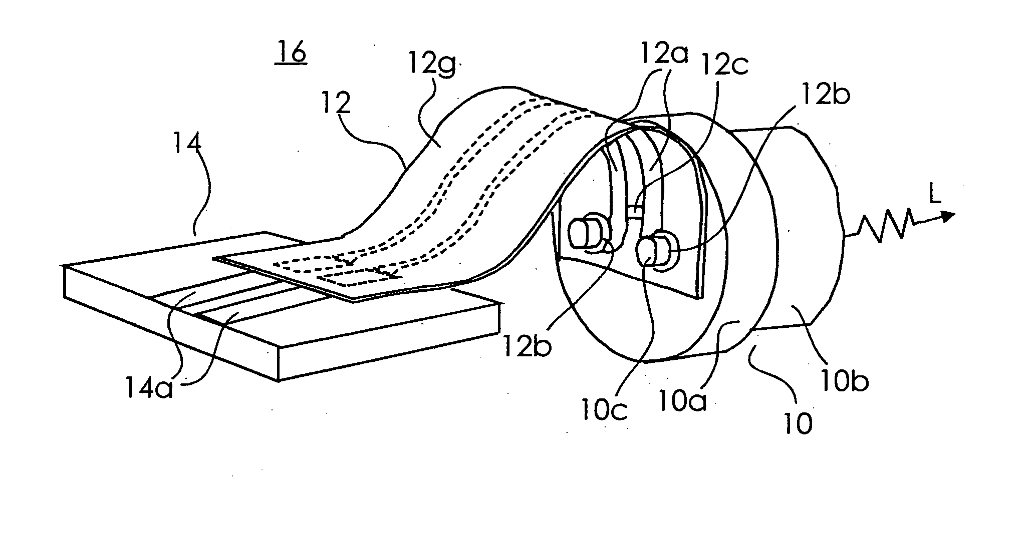
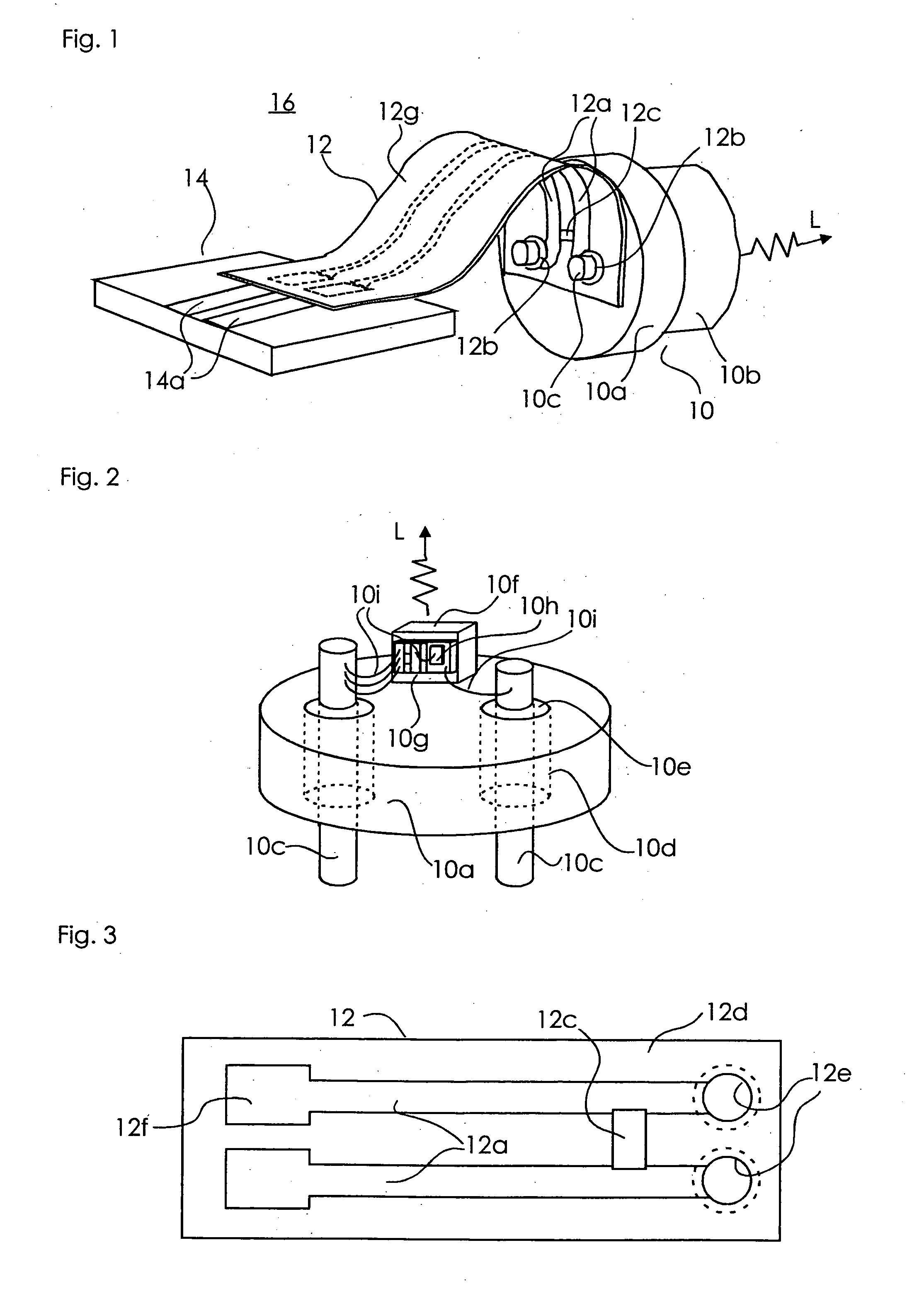
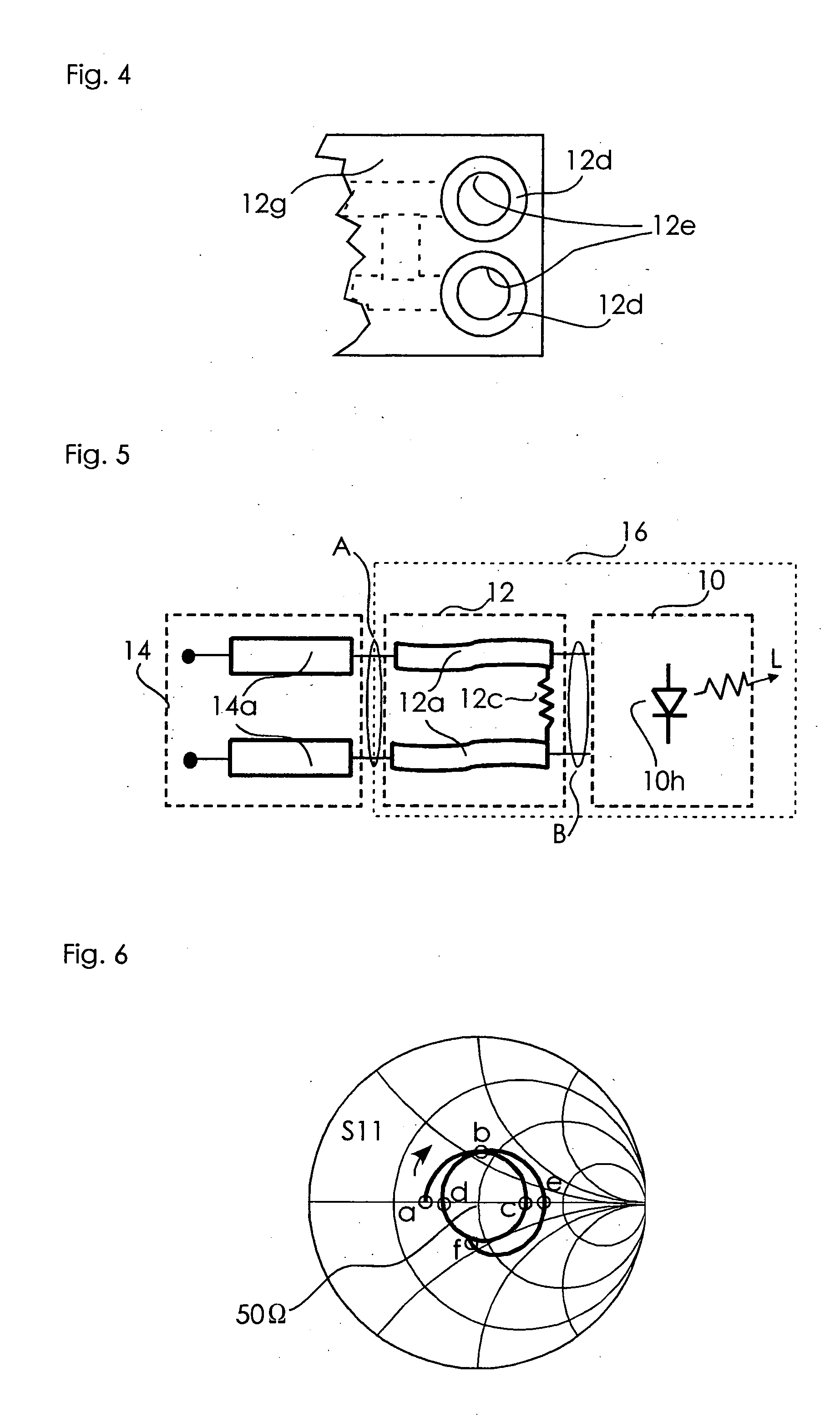
[0053]FIG. 1 is a perspective view of an optical semiconductor device according to an embodiment of the present invention; FIG. 2 is a perspective view showing the interior of a can package according to an embodiment of the present invention; FIG. 3 is a plan view of the flexible substrate according to an embodiment of the present invention observed from the front face thereof; FIG. 4 is a partial plan view of the flexible substrate according to the embodiment of the present invention observed from the back face thereof; and FIG. 5 is an equivalent circuit diagram of the optical semiconductor device shown in FIG. 1. In the drawings to be referred to below, like reference numerals will denote like or equivalent components.

[0054] Referring to FIG. 1, a can package 10 serving as an optical semiconductor package is sealed by a cap 10b that protects elements, such as a laser diode, mounted on a stem 10a serving as a substrate. Lead terminals 10c serving as electrode terminals for connec...

second embodiment

[0104]FIG. 15 is a perspective view of an optical semiconductor device according to one embodiment of the present invention. FIG. 16 is an equivalent circuit diagram of the optical semiconductor device shown in FIG. 15.

[0105] The first embodiment has referred to the example wherein the resistor 12c working as the impedance matching means is connected near the connection area B wherein the flexible substrate 12 and the lead terminals 10c of the can package 10 are connected.

[0106] A laser device 25 according to the second embodiment has the same construction as that according to the first embodiment except that a capacitor 12j is provided in addition to a resistor 12c, the capacitor 12j being connected in series with the resistor 12c. The resistor 12c and the capacitor 12j constitute the impedance matching means. In this case, the resistor 12c is, for example, a chip resistor, and the capacitor 12j is, for example, a chip capacitor.

[0107] A bias voltage of about a threshold value i...

third embodiment

[0119]FIG. 20 is a perspective view of an optical semiconductor device according to one embodiment of the present invention. FIG. 21 is an equivalent circuit diagram of the optical semiconductor device shown in FIG. 20.

[0120] The second embodiment has shown a case where the transmission lines 12a are directly interconnected through the capacitor 12j and the resistor 12c connected in series. The construction of the third embodiment is the same as that of the second embodiment except that each transmission line is connected with a grounding end through the intermediary of a capacitor 12j and a resistor 12c connected in series.

[0121] Referring to FIG. 20, in a flexible substrate 12 of a laser device 30, thin-film resistors 12c having one ends thereof respectively connected to transmission lines 12a at near through holes 12e are disposed on a polyimide film 12d, and the other ends of the individual thin-film resistors 12c and islands 12k formed of conductive films that provide the ele...


PUM


Abstract

A laser device includes a can package of a laser diode having a lead terminal secured to a through hole in a stem by a sealant, and a flexible substrate having a transmission line on a front surface of a polyimide film. The lead terminal of the can package and one end of a transmission line of the flexible substrate are connected by soldering. A resistor for matching the impedance of the transmission line and the impedance of the lead terminal is located in the vicinity of a connection of the transmission line and the lead terminal.

Description

BACKGROUND OF THE INVENTION [0001] 1. Field of the Invention [0002] The present invention relates to an optical semiconductor device and, more particularly, to an optical semiconductor device that carries high-frequency signals used for optical communication or the like. [0003] 2. Description of the Related Art [0004] In recent years, with the advancing broadband optical communication, the demand for transmitting a larger volume of information at lower cost has been accelerating concurrently with the increasingly disseminating public communication networks that use optical fibers. To increase the volume of information at low cost, it is necessary to achieve higher transmission speed. The transmission has been increased from 600 Mbps to 2.5 Gbps, and it is gradually being further increased to 10 Gbps. With this trend, light emitting devices and light receiving devices used with optical transmitters and receivers are being required to exhibit stable performance at high speed. At the s...

Claims


Application Information

Patent Timeline
IPC IPC(8): H01L23/495H01L23/12H01L25/00H01S5/022H01S5/042H05K1/02H05K1/14H05K1/18H05K3/34
CPCH01S5/02212H01S5/0427H01L2924/30107H01L2924/3011H01L2224/48091H05K2201/10121H05K2201/10022H01S5/06226H05K1/023H05K1/141H05K1/147H05K1/189H05K3/3447H05K2201/049H01L2924/00014H01L2924/00
Inventor ISHIMURA, EITARO
Owner MITSUBISHI ELECTRIC CORP
Features
  • Generate Ideas
  • Intellectual Property
  • Life Sciences
  • Materials
  • Tech Scout
  • Unparalleled Data Quality
  • Higher Quality Content
  • 60% Fewer Hallucinations
Learn More